Datasheet
Quantus Extraction Solution
Next-generation tool with the fastest performance and scalability, best-in-class accuracy using smart solvers, and in-design and signoff parasitic extraction that customers trust
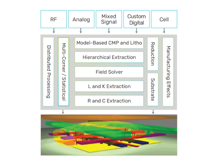
The Cadence Quantus Extraction Solution is a next-generation parasitic extraction tool for digital and custom/analog flows. Providing the fastest single-corner and multi-corner runtimes compared to other methodologies, the tool features massively parallel architecture for performance and scalability across hundreds of CPUs. Its high-accuracy modeling engine delivers impeccable, silicon-proven accuracy over thousands of tapeouts to support FinFET and all other designs. It uses one unified, foundry-qualified ”qrctechfile” for both digital and transistor-level extraction. The solution, employing a robust 3D modeling framework, is certified by TSMC for all nodes down to 2nm. In addition, the Quantus Extraction Solution is certified for all nodes at all other leading foundries.
Overview
Overview
As advanced-process geometries continue to shrink, parasitic extraction has become critical throughout the design implementation flow and the signoff phase. The Quantus solution is a production-proven signoff extraction tool ideal for all nodes, including advanced nodes and FinFET designs. The solution includes a built-in 3D capacitance random-walk field solver, Quantus Field Solver. Its objective includes modeling physical effects to ensure that extracted parasitics match those on silicon. By delivering higher accuracy parasitics, the tool helps to reduce overall design cycle times and significantly enhances the quality of silicon in complex designs. Integrated with the Cadence Innovus Implementation System and Virtuoso Studio, the Quantus solution is the most complete and efficient path to accurate parasitic extraction for all mainstream and advanced-node designs, including FinFET. Furthermore, it is tightly integrated with the Cadence Tempus Timing Solution to provide the fastest convergence and up to 3X reduction in overall timing signoff flow turnaround time. It is also tightly integrated with the Voltus-XFi Custom Power Integrity Solution for electromigration (EM) and IR drop analysis, ensuring accuracy for FinFET designs.
Key Benefits
-
 Best-in-class accuracy for FinFET designs versus foundry golden
 - 5G-ready to support all design types
- Tighter accuracy against field solver, with a near-zero mean
- Highly accurate critical net extraction with integrated Quantus Field Solver
- High performance and scalability with massively parallel architecture, supporting a linear gain when the number of CPUs used is doubled
- Scalability for single- and multi-corner extraction runs, with up to 3X faster performance in multi-corner runs
- Accurate and fastest runtimes for functional ECOs via automated incremental extraction
- Unmatched accuracy and a significantly reduced netlist that enables faster simulation and characterization runtimes for FinFET designs
- Faster and better design convergence with integration with the Innovus environment and Virtuoso ADE Product Suite
- Supports OpenAccess and hierarchical extraction for both flows
Features
- Quantus I-DSPF Output—a revolutionary debugging tool combining Interactive view and ASCII DSPF in the Virtuoso environment, delivering a faster turnaround time
- Provides enhanced interactive debugging, allowing engineers to navigate parasitic data and potential issues
- Offers real-time feedback on the impact of design changes, enabling engineers to assess and iterate seamlessly, accelerating the design debugging cycle
- Incorporates visual aids, offering designers a clearer representation of parasitic elements and their impact on the overall circuits
-
- Quantus Smart View—the next-generation Extracted View in the Virtuoso environment, delivering up to 10X best-in-class performance
- Up to 7X faster than Extracted View
- Up to 7X smaller netlist size than Extracted View
- 10X faster netlisting within the Virtuoso ADE Product Suite
- Provides key post-layout simulation verification functionality, such as in-context cross-probing, back annotation, and single Smart View for multiple process corners
- Same usability, interface, and integration to support the Virtuoso ADE Product Suite’s parasitic resimulation methodology
- DSPF file format output allows direct support for FastSPICE tools such as Spectre simulators
- Enables faster verification and simulation runtimes with Spectre X Simulator and Spectre Accelerated Parallel Simulator (APS)
-

Massively parallel technology
The Quantus solution is built with massively parallel technology to extract multi-million gate chips efficiently. The extraction tasks are distributed across multiple CPUs and/or machines for execution in parallel. Thus, the tool, which scales easily to hundreds of CPUs, can deliver a linear performance gain when the number of CPUs used is doubled.
Multi-corner/temperature extraction
With the rapidly increasing number of process corners at advanced nodes, design convergence is becoming a bottleneck in the design flow process.
For example, signal integrity issues can occur at high-temperature conditions, requiring efficient multi-corner extraction performance, including temperature corners. The Quantus solution extracts multiple corners simultaneously while significantly reducing overall runtime without compromising accuracy. In fact, the tool delivers 3X faster performance in multi-corner runs versus single-corner runs done in parallel. This functionality is available for both digital and transistor extraction flows. In fact, on the transistor extraction, the Quantus solution’s Extracted View output can support multiple process corners in one file, which allows designers to perform circuit debugging faster in the Virtuoso ADE Product Suite and improve productivity—a highly differentiated functionality.
Support for 2nm FinFET processes
The Quantus solution is fully certified for the 7nm+, 5nm, 3nm, and 2nm FinFET processes at TSMC. These process nodes introduce their own set of parasitic challenges, including multi-patterning (MPT) and accurate modeling of pillar and bridge vias in addition to other MEOL/FEOL and BEOL features. All these features have a significant impact, if not modeled accurately, on static timing analysis (STA), signal EM and IR analysis, and place and route implementation.
The Quantus solution has accurately modeled these foundry-mandated features and passed certification criteria with a tighter correlation of RCs to the foundry golden values.
Better design convergence via integration with Innovus and Virtuoso platforms
As an integral part of the silicon analysis function inside the Virtuoso custom IC design platform, the Quantus solution provides critical parasitic information for optimizing chip performance and yield.
Essentially, the extraction tool brings the physics of interconnect parasitics into the Virtuoso environment for designing, characterizing, and optimizing chip layouts. Through the tool’s integration with the Innovus environment, the designer benefits from a seamless solution for timing, IR, EM, signal integrity analysis, and power verification. Integrating the two tools reduces design turnaround time by performing incremental extraction, using integrated virtual metal fill for faster convergence, and reaching timing closure faster by using signoff-accurate extraction data for timing and noise optimization.
Tight integration with Tempus solution
At advanced nodes with multi-million instance designs, preventing parasitic load, read, and analysis turnaround time from becoming a bottleneck is critical. The Quantus solution provides a binary interface and format, RCDB, with the Tempus solution and Innovus environment. RCDB is a random-access format that reduces memory footprint. The format offers up to 120X better performance while reading in the SPEF file into the Tempus solution. In addition, the Quantus solution also offers multi-corner values SPEF, which significantly reduces output generation times, read-in times in the Tempus solution, and SPEF file size. This flow provides up to 3X overall performance improvement for timing signoff flow, i.e., extraction and STA analysis.
Tight integration with Voltus and Voltus-XFi solutions
For advanced nodes and specifically for FinFET designs, there are very complex design rules in EM checks, such as complex wire shapes, special width definition, heavy direction dependence, via shape rules for fracturing, local interconnect M0 rules, etc. It is imperative for FinFET designs for a parasitic extractor to accurately model these effects and provide resistance values for accurate EM checks. In addition to the complex design rules, there is also a self-heating-effect (SHE) flow at TSMC that requires a tighter handshake between the parasitic extraction tool and the EM-IR analysis tool. The Quantus and Voltus-XFi solutions provide such a differentiated flow to our customers to accurately perform both signal and power net EM-IR. In fact, it’s the only flow solution available in the market that provides the level of accuracy and know-how required for accurate EM and IR analysis.
Integrated Virtual Metal Fill
For 28nm and above, metal fill used to be added very late in the design cycle after timing was closed, which meant that any additional capacitance that resulted was simply ignored. This methodology is neither sufficient nor recommended for FinFET designs. Designers must consider and understand the impact of metal fill during implementation rather than waiting to insert and analyze during signoff. For example, at 40nm, the difference in capacitance of not considering metal fill during implementation and signoff was about 1%. Since then, it has grown to more than 4% for 16FF designs, and it is expected that for 10/7nm and below, the impact will be even higher. Designers started realizing this impact for their FinFET designs and began mitigating by considering metal fill during implementation—signoff metal fill. However, the net impact of this methodology had a significant impact on runtimes since signoff metal fill in GDS consumes design closure turnaround time, especially with a few ECOs in the optimization phase. The Quantus solution offers integrated virtual metal fill (IVMF) both in-design in the Innovus environment and in the standalone signoff version.
Advanced parasitic netlist reduction
One of the challenges introduced due to the introduction of FinFET designs is a huge increase in the netlist size. This bloating is due to an increase in the number of parasitics, specifically R and fin coupling cap (Cc). A new modeling layer, the middle interconnect layer or M0VO, introduces additional interconnect vias that result in an increasing number of Rs. The increase in the netlist size significantly impacts simulation runtimes, which is a costly proposition both in terms of performance and cost of acquisition. The current built-in reduction capabilities in the parasitic extraction tool needed to be enhanced significantly to meet the new challenges. The Quantus solution’s new reduction algorithm is available as a built-in capability and as a standalone version that can reduce netlist size from any third-party parasitic extraction DSPF file.
Inductance extraction for GDS and LEF/DEF flows
Clock distribution networks employ wide wire routing to span large areas of the die, which can lower clock latency and improve performance. Examples of such common routing structures are H-tree, mesh, and fishbone routing. At advanced-process nodes, clock frequencies are commonly above 1GHz with ever-faster clock edges. These exacerbate the impact of inductance by inducing overshoot and undershoot on clock waveforms and impact edge rates and shapes. Clock nets routed on thick, higher layers are driven by very strong buffers, which cause edge rates to go high, indicated by ringing in the signal due to inductance. Inductance effects bring uncertainty for hold timing and can result in chip failures. The Quantus solution is a market leader in providing an RLCK for GDS flow for transmission lines and has extended that modeling to LEF/DEF flow for SoC designs.
Advanced substrate modeling capability
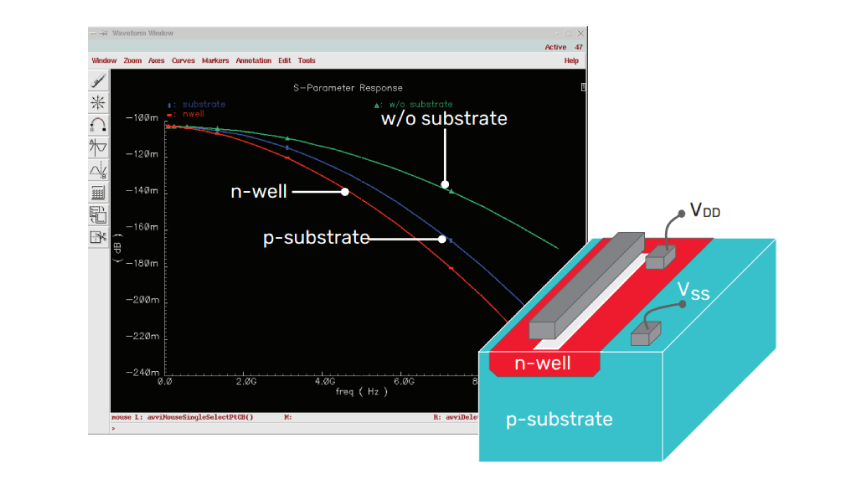
RF designers need a tool that extracts parasitic inductance accurately and evaluates the impact of substrate parasitics on their designs. Substrate noise coupling is a growing concern due to higher frequencies, higher integration, smaller feature sizes, and lower supply voltages. Including the p-substrate and n-well as part of the substrate model affects the extracted result and leads to RF interconnect loss. The Quantus solution includes a full 3D substrate model with full-chip and block-level views for accurate simulation and analysis of RFIC circuits and performs what-if analysis for substrate noise distribution.
Support for all design types
With its built-in, advanced functionality, the Quantus solution supports all design types, including custom/analog and RF, SerDes, IP/SRAM/ bitcell characterization, memory, power MOSFETs, LCD/TFT, and image sensors.
Specifications
Packaging
- Available in L and XL configurations for basic extraction
Foundry
Quantus techfiles (qrctechfile) are:
- Certified and supported by TSMC and other foundries worldwide down to 2nm
- Flow tested and qualified with foundry process design kits (PDKs)
- Complemented by development services (available from Cadence)
Format support
- Design input: GDSII, LEF/DEF, DFII, OpenAccess
- LVS data: Cadence Assura Physical Verification, Cadence Physical Verification System, Cadence Pegasus Verification System, and Mentor Graphics Calibre platform
- Design output : DSPF Interactive Output, Smart View, Extracted View, DSPF, xDSPF, SPICE, SPEF, xSPEF, SSPEF
- Direct binary interface to Tempus solution: RCDB and multi-corner value SPEF
Platforms
- Linux 64 bit
Further Information
Learn more about Quantus Extraction Solution.