Overview
Enabling Next-Generation Wireless Design
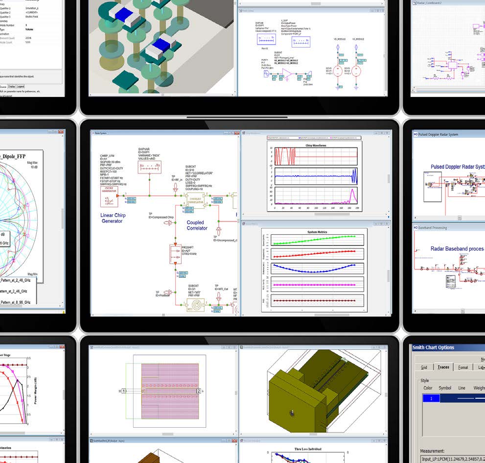
The Cadence AWR Design Environment Platform accelerates RF/microwave product development cycles with design automation that enhances engineering productivity and reduces turnaround time. This seamlessly integrated platform empowers engineers with advanced high-frequency circuit and system simulation coupled with in-design electromagnetic (EM)/thermal analyses for manufacturing-ready high-frequency IP, offering unmatched efficiency and precision.
AWR Design Environment Platform
A platform for circuit, system, and EM simulation for RF/microwave product development
Key Benefits
The Platform Advantage
Innovative User Interface
Designed to enhance engineering productivity, the user interface is powerful and intuitive. It offers smart, customizable design flows that cater to the specific needs of today's high-frequency semiconductor and PCB technologies.
Smarter Design Entry for RF/Microwave
A unified design capture system facilitates a front-to-back physical design flow. Electrical and layout design entries are dynamically linked, ensuring that components placed in an electrical schematic automatically generate a synchronized physical layout.
Comprehensive Simulation and Analysis
Nonlinear harmonic balance and circuit envelope simulation combine with in-design EM/thermal analyses to provide accurate predictions of linear and nonlinear network behavior across chip, package, and PCB. Develop component specifications from system link budgets and analyze device performance with system testbenches using modern communication standards.
Interoperability and Manufacturing Readiness
Advanced yield analysis and optimization enhance design robustness and maximum profitability. Tape out production-ready GDSII, DXF, and Gerber files directly or use the platform interoperability with Cadence Virtuoso Studio or Allegro X Design Platform to leverage powerful back-end signoff functionality.
Applications
Streamline High-Frequency Electronic Design, Optimize SWaP-C Goals, and Reduce Turnaround Time
-
Amplifiers
Accelerate RF amplifier development with robust harmonic-balance (HB) simulation for fast and accurate nonlinear circuit simulation, harmonic load-pull and nonlinear stability analysis, in-design EM and thermal analysis, and highly accurate device/circuit element models.
![Amplifiers]()
-
Antennas
Develop high-performance antennas and phased array systems for next-generation sensors, radars, and communication systems with integrated planar and 3D EM technologies, parametric optimization, and circuit co-simulation. Simulate and maximize antenna metrics such as gain, return loss, radiation efficiency, and currents, and visualize 2D/3D far-field antenna patterns.
![Antennas]()
-
Communications
Meet 5G/6G technology demands such as MIMO and beamforming antenna arrays, mmWave spectrum use, and carrier aggregation. VSS software supports time and frequency domain system-level simulation, budget and spurious heritage analysis, RF planning and end-to-end system simulation using RF and signal processing behavioral models to capture the impact of front-end electronics, channel propagation, and baseband design on digitally modulated signals.
![Communications]()
-
Filters
Designing form-factor filter solutions with low passband insertion loss and sufficient stopband rejection requires a design flow that supports filter synthesis through physical realization and verification. Cadence Microwave Office software with iFilter synthesis and Cadence planar and 3D EM technologies address all stages and types of filter development, from lumped-element or distributed filters to more complex multiplexed, high-power, and high-Q cavity filters.
![Filters]()
-
Passives
Successful design of passive components such as couplers, circulators, and attenuators focuses on reducing the device footprint, costs, and associated insertion losses. Integrated within the AWR Design Environment platform, the Cadence AXIEM 3D planar EM analysis software and Clarity 3D Solver provide fast solver technology that readily supports characterizing and optimizing passive components on RF PCBs, modules, glass and ceramic materials, and III-V monolithic microwave integrated circuits (MMICs).
![Passives]()
-
Radar and Sensor Design
Radar and sensor design evolves with advances in antenna array and semiconductor technologies. These applications are driving the need for smaller, cost-effective systems with the reliability and resolution to accurately track the speed, distance, and movement of multiple targets. Accurately representing signal generation, transmission, phased arrays, T/R switching, clutter, noise, jamming, and signal processing enables users to tackle the design challenges and analysis requirements for modern radar systems.
![Radar and Sensor Design]()
-
System Simulation Modeling
As a game changer for system development, component specification, and overall design management, VSS communications and radar systems design software lets you perform detailed link budget analysis, spurious heritage checks, and immersive time-domain simulations. With its intuitive interface, you can easily apply behavioral RF models and baseband signal processing to craft optimal system architectures. Plus, its virtual testbenches let you co-simulate key metrics like ACPR, BER, and EVM using Microwave Office software or Virtuoso design IP.
![System Simulation Modeling]()


Customer Stories
Discover Inspiring Success Stories Enabled by AWR Design Environment Platform
endorsements
See What Customers Have to Say
"[I can] lay out everything in the Cadence AWR software quickly and correctly and to send it straight to be manufactured has allowed me to complete design cycles in a short time."
Mark Greene, Qorvo
"Cadence platforms such as the AWR Design Environment, Allegro PCB/SiP, and Virtuoso RF with integrated EM solver technologies are critical to the development of our RF/mmWave MMIC, RFIC and multi-chip 2.5/3D packaging technology,”
Florian Herrault, group leader, Advanced Packaging Solutions at HRL Laboratories
“The unique, open, and integrated environment of VSS enabled us to study the effects of the nonlinear distortion on our communications link margin using real digital modulated analog waveforms.”
STEPHAN VANFLETEREN, GENERAL DYNAMICS
Capabilities
Accelerate RF/Microwave IP Development Across MMIC, RF PCB, and Module Technologies
To meet the high-performance and reduced footprint requirements for multi-mode/multi-band handsets, wireless smart devices, and aerospace systems, companies are differentiating themselves by developing best-in-class RF/microwave IP. Whether these products are compound semiconductor-based MMICs, acoustic filter laminates, or tightly integrated multi-chip modules and/or mixed-signal PCBs, designers of RF/microwave front-end electronics require specialized design and simulation from the capabilities with the AWR Design Environment Platform to meet aggressive performance targets.
Integrated EDA Platform

The AWR Design Environment Platform, with integrated Microwave Office, VSS, and Cadence multiphysics analysis tools, offers a comprehensive solution for high-frequency circuit and system design, simulation, and electromagnetic analysis, supporting all phases of high-frequency product development from synthesis to design entry, optimization, and tapeout for MMIC- and PCB-based manufacturing.
Circuit/System Simulation

The robust APLAC harmonic-balance (HB) simulator in Microwave Office software supports simulation of nonlinear RF/microwave circuits including all classes of power amplifiers operating well into compression as well as frequency converters (mixers). RF simulation technology includes load-pull analysis for determining the optimum source and load impedances to achieve key amplifier performance metrics as well as advanced nonlinear stability analysis technology to ensure that your amplifier behaves.
In-Design Planar, 3D EM, and Thermal Analysis

The AWR Design Environment platform’s EXTRACT flow provides schematic-driven, in-design multiphysics analysis for interactive full-wave method of moments (3D planar) and finite element method (arbitrary 3D) S-parameter extraction, EM-based optimization, and swept parameterization across single and multi-fabric technologies. In-design analysis includes the Celsius Thermal Solver for temperature-sensitive circuits such as heat dissipating power amplifiers and acoustic filters.
Design Aids

Filter, impedance matching, and phased array synthesis tools accelerate design starts by generating electrical networks from user-specified RF behavior criteria. Powerful automation features expedite design tasks and manage project data, including labor-saving wizards, to import PCB layout and simplify multi-step engineering tasks. The platform’s powerful application programming interface (API) and support for Python and Visual Basic programming languages, extends the capabilities of the software by allowing users to create custom scripts for automating common or complex design tasks.
Optimization and Yield Analysis
The software offers multiple fast and robust optimization algorithms to meet performance goals graphically defined on the measurement plot by the designer. The proprietary hybrid optimizer method offers a top-performing algorithm to address a wide range of RF problems. Analyze the impact of manufacturing variations, parametric material dielectric variations, and surface-mount part tolerances with yield analysis that assists the designer in identifying the parameter sets leading to yield failures.
PDK Support

RF compound semiconductor foundry process design kits (PDKs) support gallium arsenide (GaAs), gallium nitride (GaN), and indium phosphide (InP) technologies for III-V MMIC design. Cadence and partnering foundries develop and validatet PDKs of scalable electrical models, layout cells, and symbols, to use with Microwave Office, AXIEM, and Celsius technologies (thermal analysis enablement is foundry and process dependent) . PDKs include active and passive device models for simulation and layout; verification rules for design rule check (DRC), layout vs. schematic (LVS), process technology data, and other foundry attributes to ensure first-pass design success.
Products
Microwave Office/VSS E-series for RF/microwave component and system product development
Microwave Office Linear
Microwave Office Linear supports design of RF passive components such as filters, couplers, and attenuators, as well as active devices operating under small-signal (AC) conditions such as low noise and buffer amplifiers. The linear configuration provides simulation of S-parameters (Y/Z/H/ABCD), small-signal gain, linear stability, noise figure, return loss/voltage standing wave radio (VSWR), and more, as well as real-time tuning, optimization, and yield analysis.
All E-series Microwave Office portfolio includes synchronous schematic / layout editors, 2D/3D viewer, comprehensive libraries of high-frequency distributed transmission models, and surface-mount vendor component RF models with footprints, measurement-based simulations, and RF plotting.
Try Today
Microwave Office PCB
Microwave Office PCB enables linear and nonlinear RF circuit design with the robust APLAC HB simulator and its powerful multi-rate HB, transient-assisted HB, and time-variant (circuit envelope) simulation engine, supporting analysis of large-scale and highly nonlinear RF/microwave circuits, such as power amplifiers and mixers (frequency converters). State-of-the-art load-pull analysis with harmonic and video-band tuning generate performance contours including available output power, gain, power-added efficiency (PAE), two-tone intermodulation distortion, and other key amplifier metrics used in the development of input/output matching circuits for optimum performance.
Try Today
Microwave Office MMIC
Microwave Office MMIC offers a front-to-back MMIC design flow with an innovative user interface and complete integration of design entry, simulation, and physical design tools that enhances engineering productivity and ensures first-pass success with PDKs from a wide range of GaAs, gallium nitride GaN, silicon germanium (SiGe), and CMOS foundry partners. The hierarchical framework supports simulation of diverse MMIC, RFIC, and PCB processes, multi-layer interconnects, embedded passives, and surface-mounted mini-devices found within multi-chip RF modules.
Try Today
VSS System
VSS System allows design teams to conceptualize and rapidly implement virtual 5G/6G and IoT communication and radar/electronic warfare (EW) systems, investigate new architectures, and study individual component or overall system performance. Design RF-aware systems and perform rigorous link budget design or spurious heritage analysis with RF/microwave behavioral models that incorporate linear and nonlinear performance metrics as well as terminal impedances which can lead to power loss due to component-to-component impedance mismatch. Combine with signal processing blocks to cover end-to-end system performance and communication testbenches for co-simulation with Microwave Office software and/or Virtuoso IP.
Try Today
Microwave Office Add-On Options
Offering a range of advanced add-on options to enhance your EM and thermal analysis capabilities.
Try Today

features
Accelerate Development of High-Frequency Electronics
Design and analyze MMICs, RFICs, RF PCBs, microwave modules, antennas, communication systems, radar systems, and more
| Feature name | Description |
|---|---|
| Design Entry | Unified data model supports concurrent schematic/layout design entry and component property editing from either schematic or layout views |
| Cadence APLAC HB Simulator | Proprietary multi-rate HB engine provides robust linear and nonlinear frequency-domain circuit simulation |
| Load Pull Analysis | State-of-the-art load-pull analysis and design support for optimum nonlinear PA performance |
| Stability Analysis | Linear and nonlinear stability analysis |
SHOW ALL
4 of 8
resources


Support
Need Help?
Cadence Support puts the help you need within easy reach – around the clock, seven days a week. Locate the latest software updates, case and Cadence change request information, technical documentation, articles, and more.
We offer two tiers of support, Basic for those focused on self-service, and Premium for those who want access to of Cadence Expert-level assistance from our team of support Application Engineers.
| Features | Basic Support | Premium Support |
|---|---|---|
| Access to Cadence Online Support (COS) Portal | ||
| Online Training Content Access | ||
| Forum Access | ||
| Bug Reporting | ||
| Incremental Updates (Bug Fixes) | ||
| AE assistance/Case Filing | ||
| Access to File a Case | ||
| Major Releases |