利用硅签核和验证的工具,设计人员可以在流片前完成一系列必要的电气及物理签核的验证步骤。这些流程可以分析报告出需要进行迭代和增量修复的问题(也称为 (ECO)),以便从电气和物理的角度确保设计完整性。
设计人员在设计复杂的系统级芯片时主要面临三个挑战:
- 性能和容量 – 签核工具运行耗时过长并占用太多内存
- 精确度 – 随着制造工艺向深亚微米节点发展,需要在早期综合时就估算并匹配签核时候的时序、布局和功耗,这将是一个更大的挑战。
- 设计收敛 – 传统时期,签核工具只能报告设计问题,但在发现问题后无法对其进行实际修复。这导致在后端实现和签核之间来回往复工作,大大延误了产品上市时间
在 Cadence,我们意识到需要加快最后一步的收敛周期,使您能够大大减少迭代次数,直至完成流片。同时,我们也意识到这些流程的执行需要足够的快。为此,我们设计了一套具有以下优点的总体解决方案:
大规模并行的云端解决方案
我们的签核工具 Quantus™ Extraction Solution、Tempus™ Timing Signoff Solution、Voltus IC Power Integrity Solution 和 Pegasus™ Verification System 均已支持云上使用,可以在大规模并行服务器群上运行。这些服务器群可以位于公司内部,也可以位于外部云提供商处。您的设计将自动划分为较小的电路单元,在多台计算机和 CPU 之间进行拆分,利用多线程技术,然后通过自适应调度来平衡计算机和 CPU 之间的负载。我们已经有数家客户正在使用这些新工具,并且见证了性能实现几个数量级的提升。
集成引擎,用于实现正确度和更快的设计收敛
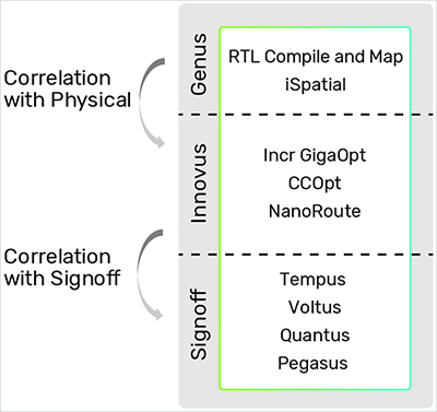
Cadence® digital design flow集成引擎目前集成了时序、布局、功耗和寄生参数提取。从Genus™ Synthesis Solution 到 Tempus 和 Quantus solutions的硅签核、Pegasus system、Design for Manufacturability (DFM) solution (DFM) 以及 Voltus™ power solution。这一流程被称为“设计在线同步验证”,可利用同步签核验证方案来避免后端实现和验证前后一致性问题——这些问题会在流片前的最终阶段令设计人员头痛不已。例如,这意味着当 Genus solution在设计周期的早期运行综合时,将使用与 Innovus™ Implementation System 在实现过程中使用的相同布局和布线,并且可以在设计周期的早期做出更好的选择,从而更轻松的修复问题。而且,在 Innovus 系统中,设计人员可以运行 Tempus Timing 和 Voltus Power solutions,以在流片时更快地实现时序收敛。这有助于显著减少设计后期的迭代次数,并加快签核期间的收敛。这种具有集成引擎的设计时能力还可以消除或大大减少设计人员对于预算的担忧,从而大幅改善设计过程中的功耗、性能和面积 (PPA)。
发现问题后及时修复问题的工具
我们的签核工具中的集成引擎不仅可以在设计流程的早期分析问题,还可以根据需要进行修复,借此显著减少实现和签核之间的来回迭代次数。我们的工具可以发现问题,分析各种情况,选择可用的最佳 PPA 优化,并在设计流程的早期进行实现,从而使设计结果接近PPA 流片最终签核指标的偏离值 2% 到 5%之内。
数字模拟混合设计和定制设计支持
所有 Cadence 签核工具或功能都集成在 Virtuoso® 平台,为数字模拟混合信号和定制设计提供相同的功能。
硅签核和验证是在每个设计流程中进行签核的最后一个关键步骤。结合使用 Cadence 设计流程与我们的集成引擎和大规模并行工具,将使这一流程进行得更加顺畅,并可以通过更出色的 PPA 目标来确保设计能够更快完成。
Our 7LPP process provides the best power, performance and area that we have seen so far in advanced FinFET nodes, and we expect this will provide great benefits for our mutual customers’ next generation SoC designs.
Ryan Sanghyun Lee, vice president of the Foundry Marketing, Samsung Electronics
We’ve verified that the Cadence methodology meets our accuracy, frequency, power and cell utilization requirements. The certification of the Cadence digital tool suite allows our mutual customers to reach their PPA targets and to experience the benefits associated with the GF 22FDX body bias techniques ...
Richard Trihy, senior director, design enablement, GLOBALFOUNDRIES
4. The Voltus IC Power Integrity Solution provided several efficiencies that enabled us to shorten the time to design closure on our largest ever switch-chip FinFET design so that we can stay in front of the competition. Given our successful, accurate silicon results, we’re planning to use Voltus ...
Sanjay Kumar, senior director ASIC Designs, Juniper Networks