Key Benefits
- Cost-effective system scaling to increase system bandwidth
- Decreases power consumption and device form factors
- Ideal solution for mobile and Internet of Things (IoT) applications
InFO Packaging Technology with Cadence Implementation Technology
Integrated design flow using Cadence IC-level and package design tools to provide a seamless flow with enhanced features for InFo technology, reducing overall design turnaround time
Cadence is enabling the successful broad deployment of TSMC’s Integrated Fan-Out (InFO) packaging technology using:
- Cadence® Physical Verification System (PVS)
- Allegro X Advanced Package Designer
- Allegro X Advanced Package Designer Silicon Layout Option
- Sigrity™ IC package analysis and 3D modeling
- Voltus™ IC Power Integrity Solution
What Is InFO Technology?
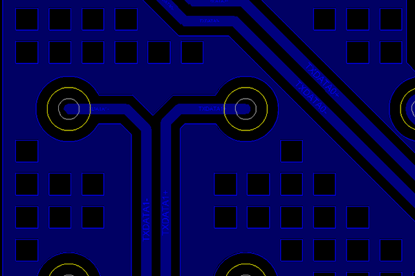
TSMC’s InFO technology is a fan-out, single, multi-die, or PoP (package-on-package) wafer-level chip-scale packaging technology that provides lower thermal resistance, excellent RF material properties, and extremely thin-layer thicknesses to meet the demands of customers who need thin devices or device stacks, optimized performance, and lower cost for mobile computing products.
What Makes InFO Technology Different from a Designer’s Perspective?
- Tightly controlled, localized metal density to provide a very, very thin package substrate
- TSMC leverages their IC artwork expertise, toolset, and flow to manufacture these devices
Enabling Technologies
To enable the TSMC customer to meet these requirements, Cadence provides:
- Ability to scan, assess, and modify the localized metal density on each layer of the design to meet the stringent density requirements for InFO technology
- Tighter integration between the IC packaging design tools and signoff PVS DRC/LVS to shorten the design cycle time
- Cell-level power integrity tool that supports comprehensive electromigration and IR-drop (EM-IR) design rules and requirements while providing full-chip system-on-chip (SoC) power signoff accuracy
Training and Support
Need Help?
Training
The Training Learning Maps help you get a comprehensive visual overview of learning opportunities.
Training News - Subscribe
Online Support
The Cadence Online Support (COS) system fields our entire library of accessible materials for self-study and step-by-step instruction.
Request SupportTechnical Forums
Find community on the technical forums to discuss and elaborate on your design ideas.
Find Answers in cadence technical forums