Key Benefits
- Production- and foundry-proven flow with multiple tapeouts
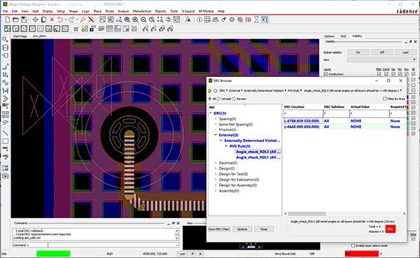
- Direct integration with PDK-driven PVS DRC/verification provides graphical designer feedback minimizing path to tapeout readiness
- Advanced WLP-specific metal creation and management removes/reduces eco spins
- High-performance GDSII processing shortens path to tapeout readiness
The Cadence® Allegro® Package Designer Plus Silicon Layout Option works with the Cadence Physical Verification System (PVS) to deliver flexible silicon substrate and advanced wafer-level packaging (WLP) design capabilities. It offers process development kit (PDK)-driven design rule checking (DRC), density modification and assessment, connectivity verification, and mask artwork signoff. Suitable for designs based on emerging silicon and wafer-based packaging methodologies, the option has been validated by TSMC for its Integrated Fan-Out (InFO) process.
The Silicon Layout Option in conjunction with PVS enables designers to address the fabrication challenges of:
- Adherence to a PDK from a foundry or silicon-based WLP manufacturer for DRC, verification, and mask signoff
- PDK-required silicon-specific interconnect (metal) density management by multiple methods to control fabrication warpage
- Silicon-based DRC spacing, manufacturing, and density checks using silicon-based rule decks
- High-performance GDSII mask-artwork processing and generation optimized for packaging design structures
- 2D and 3D extraction, modeling, and analysis for signal integrity (SI) and power integrity (PI) performance and stability (through optional Cadence Sigrity™ technology)
- Complying with silicon substrate manufacturing artwork rules
The option has been part of production- and foundry-proven flows with multiple tapeouts. A direct integration with PDK-driven PVS DRC/verification provides graphical overlay and table-formatted feedback on the Allegro Package Designer Plus canvas, minimizing the path to tapeout readiness.
NOTE: The Cadence Physical Verification System (PVS) is mandatory for silicon and wafer-level design flows but must be purchased seperately.
Training and Support
Need Help?
Training
The Training Learning Maps help you get a comprehensive visual overview of learning opportunities.
Training News - Subscribe
Online Support
The Cadence Online Support (COS) system fields our entire library of accessible materials for self-study and step-by-step instruction.
Request SupportTechnical Forums
Find community on the technical forums to discuss and elaborate on your design ideas.
Find Answers in cadence technical forums