Brochure
40Gbps D2D PHY IP for TSMC 5nm FinFET
Overview
Overview
Today’s emerging hyperscale data centers and a new breed of accelerator / artificial intelligence / machine learning (AI/ML) applications are creating the need for increased per-socket compute power, high bandwidth, low power, and low latency. The Cadence 40G D2D PHY IP provides an alternative to the high cost of on-die integration, as it caters to growing system-in-package (SiP) applications: CPU to CPU in a multi-core SoC, low-latency coherent interconnect, DSP arrays to process information from lidar, switch fabric integration on multi-chip module (MCM), network ASIC to SerDes PMD on separate die, and chip to in-package optical engine.
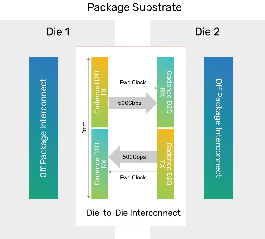
The Cadence 40G D2D PHY IP delivers up to 40Gbps wire speed in an NRZ serial interface, providing up to 1Tbps/mm unidirectional bandwidth. The IP includes built-in de-skew and scramble/de-scramble logic to enable easy system integration. Its low wire count of 28 data wires for 1Tbps bandwidth enables easier routing and potentially reduces package cost, whereas alternative solutions can require 30% or more wires. While some existing lower speed die-to-die solutions require a silicon interposer to achieve the same bandwidth, the Cadence D2D PHY IP offers significant cost advantages by supporting MCMs on organic substrates. This IP features low latency as low as 5ns rount trip from receiver to transmitter, utilizes standard non-return-to-zero (NRZ) coding, and achieves better than 10-15 bit error rate (BER) without requiring forward error correction (FEC).
Benefits
-
 1Tbps/mm unidirectional bandwidth
 - Low power and low latency
- Easy routing and straightforward integration
- Supports MCMs on organic substrates
- Better than 10-15 BER without requiring FEC
Key Features
- Flexible data rate up to 20Gbps to 40Gbps
- Single-ended NRZ signaling scheme
- BIST features to ensure “known good die”
- Sideband for link management
- Inter-operable between different technology nodes and foundry
Product Details
The Cadence 40G D2D PHY IP consists of a transmitter (TX) macro and a receiver (RX) macro.
TX Macro
The TX macro consists of a 7-wire interface supporting 20 to 40Gbps serial line rate per wire. Its variable line rate provides 120 to 240Gbps un-encoded throughput. Tiling is supported to achieve higher throughput. The TX macro utilizes singleended signaling. A low-jitter embedded phased-lock loop (PLL) provides a sub-rate internal clock and forwards the clock to the far-end RX.
RX Macro
Similar to the TX macro, the RX macro also consists of a 7-wire interface supporting 20 to 40Gbps serial line rate per wire and 120 to 240Gbps total un-encoded throughput. Tiling is supported to achieve higher throughput. The RX macro supports automatic self-calibration at start-up, which uses pre-selected calibration patterns from the TX group for calibration of RX analog “lanes”.
BIST
Both RX and TX macros support link built-in self-test (BIST) pattern checking for testing the complete data path through a TX/RX group. Per-lane BIST supports PRBS7, PRBS15, PRBS23, PRBS31, and user-defined pattern checkers. Analog Test Bus is available for test and characterization.
Clocking and Reference Clocks
The TX macro takes the 100MHz reference clock input and generates high-speed differential clock output to forward to the RX macro. The RX macro uses the high-speed differential clock input of forwarded clock from the TX group to recover data.
Deliverables
- Verilog simulation models (digital RTL and analog behavioral)
- Verilog testbench with example run scripts, demonstration tests, and bus functional models
- Full documentation set including integration, user, and programmer guides
- DFT collateral including ATPG generation and setup guidelines and scan abstracts (CTL)
- IPXACT register abstracts
- Liberty timing models (NLDM with and without LVF)
- LEF physical abstracts
- Verilog gate-level netlists (power-aware and non-power -aware) with full set of SDF back-annotation data
- GDSII physical databases with physical verification reports (LVS, DRC)
- IBIS models for serial I/O
- Current profiles
- High-volume manufacturing test environment and test suite
For more information, visit Design IP.