Improve Manufacturability with CMP-Friendly Design
LOG IN TO VIEW PRESENTATION
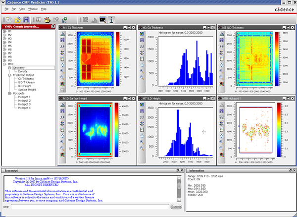
The Cadence® Pegasus™ CMP Predictor predicts chemical and mechanical polishing (CMP) variations and their potential impact on your design for the entire layer stack. It turns the uncertainty of manufacturing process variation into predictable impacts and then minimizes these impacts during dummy fill definition and at the design stage to greatly enhance overall design performance and yield. Traditionally used at the chip level, Pegasus CMP is also applicable at the IP level with its unique block-based methodology and at the wafer level with advanced wafer-scale modeling and prediction. Pegasus CMP provides wafer-scale, full-chip, multi-level thickness and topography predictions for the entire stack, covering FEOL, MOL, and BEOL deposition, etch, and planarization processes.
CMP-related hotspots, such as copper pooling, can have detrimental effects on wafer and chip yield. The conventional rules-based approach to hotspot detection fails to capture long-range and multi-level CMP effects. Pegasus CMP uses a highly accurate model-based approach to find potential hotspot areas. It also feeds the thickness and topography variation data into extraction tools, enabling better RC and timing analysis. The Pegasus CMP thickness and topography variation output is also used to compare different dummy fill strategies and to optimize dummy fill approaches.
Pegasus CMP integrates with the Cadence Virtuoso® Layout Suite and Cadence Innovus™ Implementation System, and interfaces closely with the Cadence Quantus™ Extraction Solution for a complete silicon signoff solution.
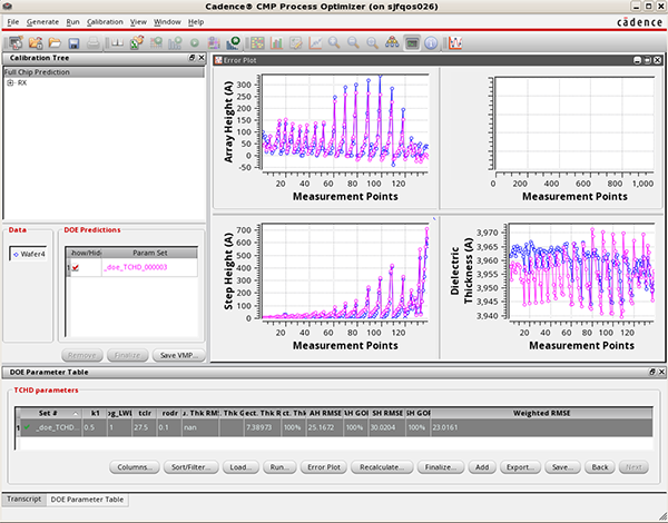
Pegasus CCPO is used by CMP, process, DFM, or PDK teams to develop CMP models used by Pegasus CMP. The model calibration is done from silicon thickness measurements and creates semi-physical models that accurately model silicon trends and topography variations. Pegasus CCPO has dedicated versions and modeling capabilities for deposition, etch, and planarization processes in FEOL, MOL, and BEOL. Pegasus CCPO supports many advanced CMP process features such as reverse etch back and deposition angle, as well as specialized process flows such as those used in CMOS image sensors, 3D NAND, copper-to-copper packaging, or other 3D-IC manufacturing. It now also includes wafer-level calibration and prediction capabilities.
With prediction and optimization capabilities at chip and wafer-level, Pegasus CCPO is used by CMP process and product teams to detect potential hotspots or yield limiting issues in new products coming to the manufacturing line, and to optimize the CMP process parameters for a specific product layout. Pegasus CCPO improves the CMP efficiency and yield for each product at the chip or wafer level.

The Cadence massively parallel architecture allowed us to significantly reduce the time spent in signoff analysis, implementation, and closure so we could quickly deliver a quality reference design to market.
Shih Chin Lin, Senior Division Director, IP Development and Design Support Division, UMC
Working together with Cadence, we’re driving advances in CMP process performance.
Derek Witty, Vice President and General Manager, CMP Products Group, Applied Materials
After an extensive evaluation of all vendors in the market, we selected the complete Cadence DFM set of technologies for our most advanced ASIC and SoC designs.
Hiroshi Ikeda, Director of the System LSI Technology and Design Platform Development Department, Fujitsu Semiconductor Limited
Training and Support
The Training Learning Maps help you get a comprehensive visual overview of learning opportunities.
Training News - Subscribe
The Cadence Online Support (COS) system fields our entire library of accessible materials for self-study and step-by-step instruction.
Request SupportFind community on the technical forums to discuss and elaborate on your design ideas.
