Webinar
Chip-Level Electromagnetic Crosstalk Signoff Using EMX Solver

Today’s wireless and high-speed chip designs integrate an incredible amount of functionality on very small silicon real estate. Such integration requires optimization from the early stages of the design to post-layout vs. schematic (LVS) signoff. Increasingly complex designs and advanced process nodes test the limits of electromagnetic (EM) solvers in terms of modeling capacity and times.
This session will present a seamless, “EM-aware” design flow. The flow starts with the synthesis and optimization of passive components using EMX Designer, followed by floor-planning optimization with “EM in the loop” analysis of coupling effects using the EMX Solver’s black-boxing feature. These topics have been covered in previous webinars. This webinar focuses on chip-level signoff of EM crosstalk.
Key takeaways:
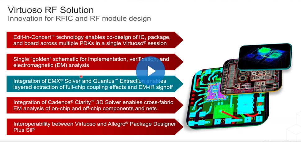
- Use a seamless, unified design flow within Cadence Virtuoso to model RC plus EM parasitics, combining EMX Solver for EM with Quantus for RC
- De-risk your design from unwanted EM coupling effects
- Achieve chip-level, “EM-aware” designs and signoff for EM crosstalk