Brochure
LPDDR5/4X PHY IP for TSMC 7nm
Overview
Overview
Today’s consumers generate and consume large volumes of data and video, exploding the need for data-intensive processing requiring high memory bandwidth. The Cadence Denali PHY IP for LPDDR5/4X for the TSMC 7nm Process is a family of high-speed on-chip interfaces to external memories, supporting these high-performance requirements with products that are optimized for each application’s needs.
The LPDDR PHY IP is comprised of architectural improvements to its highly successful predecessor, achieving breakthrough performance, lower power consumption, and smaller overall area. The application-optimized LPDDR PHY IP can achieve speeds up to 6400Mbps. Low-power features include the addition of a VDD low-power idle state in the PHY and power-efficient clocking during low-speed operation for longer battery life and greener operation. Redesigned I/O elements reduce overall area by up to 20%.
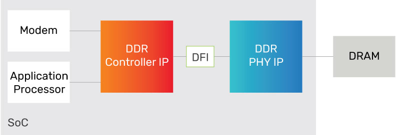
The LPDDR PHY IP is developed by experienced teams with industry-leading domain expertise and extensively validated with multiple hardware platforms. It is engineered to quickly and easily integrate into an SoC, and is verified with the Denali Controller IP for DDR as part of a complete memory subsystem solution. The LPDDR PHY IP is designed to connect seamlessly and work with a third-party DFI-compliant memory controller.
Benefits
-
 Lowest latency for data-intensive applications
 - Highest data rates with detailed system guidelines
- Maximum system margin with advanced clocking and I/O architectures while reducing power and area
Product Details
The LPDDR PHY IP consists of a DFI interface to the memory controller, external register interface (configuration and test), PHY control block (initialization and calibration logic), and configurable data slices. The LPDDR PHY IP is a highperformance DQS-delay architecture that uses programmable clock delay lines to align write data, read data capture, and DQS gating from the I/O pads across the DFI interface to the memory controller.
Key Features
- Application-optimized configurations for fast time to delivery and lower risk
- Memory controller interface complies with DFI standard up to 5.0
- Internal and external datapath loop-back modes
- Per-bit deskew on read and write datapath
- Low-power VDD idle, VDD light sleep, and power-efficient clocking in low-speed modes
- I/O pads with impedance calibration logic and data retention capability
- RX and TX equalization for heavily loaded systems
- Fine-grain custom delay cell for delay tuning
PHY Architecture
To optimize the DDR interface implementation, the LPDDR PHY IP provides complete flexibility with process, library, floorplan, I/O pitch, packaging, metal stackup, routing, and other physical parameters. The LPDDR PHY IP is implemented with a slice-based architecture that supports a wide range of memory classes and data rates.
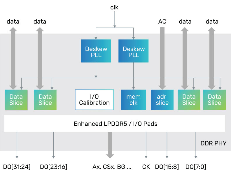
Data Slice and Address/Control Slices
The data slice is an 8-bit-wide design that interfaces to the DQ, DM, and DQS connections of the DRAM. The data slice is duplicated to create the appropriate data width, allowing flexibility to adjust to meet the requirements of the systems or applications.
The address and address/control slices interface to the control, command, and address connections of the DRAM. The address and address/control slice is duplicated to create the appropriate width for different protocols or combination of protocols, allowing flexibility to adjust the number of control, command, and address signals as needed.
External Register Interface
The external register interface is a Cadence-proprietary interface to access the data slice registers.
PHY Control Block
The LPDDR PHY IP control block provides initialization and calibration logic for training the DQS alignment for each data slice.
Availability
The LPDDR PHY IP is available with various configurations and supports the following protocols:
| Protocol | Speed | Process Node |
|---|---|---|
| LPDDR5/4X | HS-6400 | TSMC N7 |
| LPDDR5/4X/4 | HS-5500 | TSMC N7 |
Related Products
- Denali Controller IP for LPDDR5/4X/4
Deliverables
- GDSII macros with abstract in LEF
- Verilog post-layout netlist
- STA scripts for use at chip or standalone PHY levels
- Liberty timing model
- SDF for back-annotated timing verification
- Verilog models of I/O pads, and RTL for all PHY modules
- Verilog testbench with memory model, configuration files, and sample tests
- Documentation, including integration and user guide, release notes
- Verification IP set-up files
For more information, visit Design IP.