Addressing the Challenges of Serial Link Design and Analysis
WEBCAST
With the exponential increase in consumer/IoT devices, zettabytes of data are being transferred each year and system designs are typically asked to double transfer speeds every two years. PCI Express® (PCIe®) is expected to move from 8Gbps to 16Gbps with version 4.0. Beyond that, some speculate that 25Gbps and greater signaling will be achieved with multi-level signaling such as PAM-4.
These increasing speeds mean designing a high-speed serial link can no longer be delegated to the expert in the lab running a 3D field solver from 1997. Multi-gigabit serial link design and analysis must find its way to the engineer’s desktop.
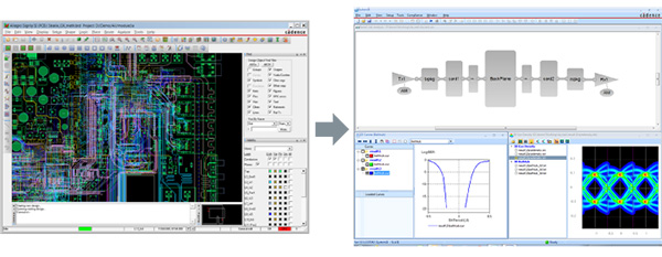
At Cadence, we are developing technology that helps you analyze and optimize all sections of the serial link. The transceivers and all the interconnects linking the chips, packages, boards, and connectors can be modeled and simulated to confirm that the serial links in your product will perform to specification.
Sigrity™ Transistor-to-Behavioral Model Conversion (T2B™) creates the analog front-end of an IBIS model from transistor-level models.
Sigrity SystemSI™ technology creates the algorithmic portion of the IBIS-AMI model in the form of a dynamic linked library that links to IBIS-compliant channel simulation engines
Sigrity XcitePI™ Extraction for chip-level extraction of signal power and ground interconnect from the I/O to the bump with header information enabling push-button connectivity to the extracted package model.
Sigrity XtractIM™ technology and 3D-EM technology work together to create a complete package model regardless of package type, for coupled signal, power, and ground interconnect models. Also included is package assessment, bridging the gap between the package designer and package characterization engineer.
Sigrity PowerSI™ technology and 3D-EM technology work together to extract coupled signal, power, and ground from PCBs. Included in the extracted model is header information enabling push-button connectivity to the extracted package model(s) and/or connector model(s).
Sigrity SystemSI technology provides easy connectivity of power-aware IBIS models with their equalization routines in IBIS-AMI format and power-aware interconnect models. Simulation results exhaustively determine worst-case conditions and compare those results to serial link interface compliance requirements such as USB or PCI Express, allowing you to sign off serial link channel design.
Training and Support
The Training Learning Maps help you get a comprehensive visual overview of learning opportunities.
Training News - Subscribe
The Cadence Online Support (COS) system fields our entire library of accessible materials for self-study and step-by-step instruction.
Request SupportFind community on the technical forums to discuss and elaborate on your design ideas.


