Datasheet
Cadence Virtuoso DFM
In-design manufacturing signoff at advanced nodes
Cadence Virtuoso DFM gives designers the ability to accurately assess the design’s manufacturability for both physical and electrical variability for custom and mixed-signal designs, libraries, and IPs. Designers can now achieve speedy silicon convergence—without ever leaving the Virtuoso Layout Suite environment.
Overview
Advanced-Node Manufacturability And Variability Yield Loss
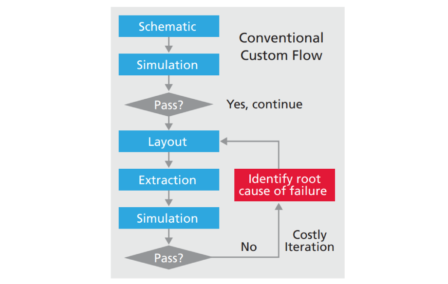
At the 45nm technology process, foundries have added mandatory DFM checks to address lithography, etch, and mask systematic-manufacturing variations that surpass random variations as the prime limiters to catastrophic and parametric yield loss. The interaction of manufacturing shapes within the optical proximity halo and the lithography projection systems creates highly non-linear systematic variations at different process conditions that cannot be captured by a rules-based approach. The minimum design rule check (DRC) rules fail to capture many potential yield issues, while relaxing DRC rules causes an unacceptable increase in design area. These systematic shape variations are dependent on specific layout-shape context, and result in predictable catastrophic errors such as necking (opens) and bridging (shorts). These yield-limiting patterns must be detected and fixed prior to tapeout.
When design teams migrate to advanced integrated circuit (IC) process nodes to increase performance while reducing area and power, layout-dependent effect (LDE) variability can compromise the timing, performance, and predictability. LDE variability caused by stress, litho, and well-proximity effects change transistor electrical performance and can only be detected after layout completion, parasitic extraction, and simulation. This is because there is no feedback during the layout-creation process between the different tools, leading to costly iterations and parametric yield loss. Most IC design teams handle LDE-induced variability by simply applying guardbands. Starting at 45nm to 40nm process nodes, comprehending DFM goes from a “nice-to-have” to a “musthave” and is a mandatory step in the IC design flow. Due to the increasing design cost and time-to-market pressure, a redesign or a few weeks’ delay because of poor yield could lead to the financial death of a project or losing a market-window opportunity.
In-Design DFM Experience For Custom Flow Implementation
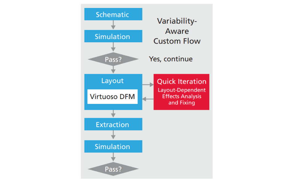
To meet the design-for-manufacturing (DFM) requirements of advanced nodes, Virtuoso DFM delivers groundbreaking in-design DFM technology in the Virtuoso Layout Suite cockpit. Virtuoso DFM provides detection and automated optimization of physical and electrical variability so custom and library designers can easily meet foundry mandatory checks.
This Cadence solution integrates award-winning, foundry “golden” technologies enabling the fastest deterministic path to DFM convergence for custom designers’ silicon realization. Virtuoso DFM preserves design intent (such as electrical constraints), achieves fast convergence through accurate abstraction, and provides highly convergent results through near-linear scalability and automatic fixing of errors. This enables engineers to implement a “correct-bydesign” flow for their leading-edge designs, efficiently and predictably, to multiple foundry partners.
Virtuoso DFM allows designers to identify, analyze, and automatically optimize the design on chip parameters for the impact of physical effects such as lithography, mask, OPC, etch, and RET; as well as layout-dependent effects such as litho, overlay, context-dependent stress, strain, well proximity, unintentional stressors like shallow-trench isolation, contact-to-contact spacing, and more. In addition, the Virtuoso in-design methodology provides an accurate, model-based flow for designers to minimize the impact of manufacturing variations on design performance.
Benefits
In-design DFM and predictable DFM closure for custom-design implementation
-
 Provides fastest deterministic path to physical and electrical DFM variability convergence
 - Enables ease-of-setup and ease-of-use
- Offers flexibility to choose DFM signoff technology depending on technology node and foundry partner
- Provides seamless error reviewing and automatic fixing of errors within the Virtuoso environment
- Enables convergent automated fixing with on-the-fly, post-fix checks
- Improves systematic and parametric yield and chip performance by accurately determining the impact of systematic variations during design
Production-proven “golden” pattern matcher for in-design DRC+ for GLOBALFOUNDRIES 28nm
- Uses foundry-certified library of yielddetractors or customer-specific yielddetractor pattern library
- Quickly detects litho-unfriendly patterns or yield detractors and automatically fixes litho violations
- Applies recommended DFM rules locally to matched areas
- Delivers convergent silicon realization in-design with multiple fixing heuristics
- Provides incremental recheck after fixing
Foundry-golden, comprehensive, modelbased litho hotspot analysis
- Quickly detects litho hotspots
- Automatically fixes litho violations and performs incremental rechecks/fixes
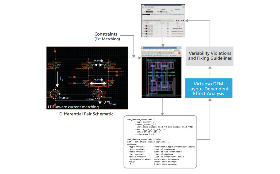
Industry’s first in-design, constraintdriven layout-dependent-effects variability detection and optimization
- Static checks detect large current or Vt variations due to LDE, without running extraction or simulation
- Generated guidelines drive layout modifications
- Supports Cadence proprietary and third-party litho and stress modeling
- Enables designer to verify that the layout meets intended matching constraints while layout is being constructed
- Integrates with Cadence QRC Extraction for contour-based transistor extraction
Boosted productivity and predictable tapeout schedules
- Near-linear multi-CPU scalability enables fastest time-to-convergence
- Hierarchical methodology ensures easy path for engineering change orders (ECOs)
- Performs incremental and what-if analysis and exploration
Features
Golden pattern matching and model-based litho hotspot engines
Traditional approaches to dealing with manufacturing variations are no longer adequate. DRC alone does not prevent catastrophic yield loss due to systematic shape variations. In addition, DRC rules to address growing DFM issues become prohibitive in number and complexity. Post-GDSII OPC uncovers printability problems that frequently require actual design changes when there is limited freedom after tapeout, making design closure unpredictable. Designers can restrict their design style in an attempt to improve yield, but this method limits the use of leading-edge processes that optimize area and performance.
For advanced nodes to achieve the fastest path to DFM convergence, designers need the flexibility to choose technologies ranging from pattern matching, hybrid litho analysis to full model-based litho analysis. Virtuoso DFM incorporates these three types of analyses.
In-design DRC+ and litho hotspots analysis and fixing
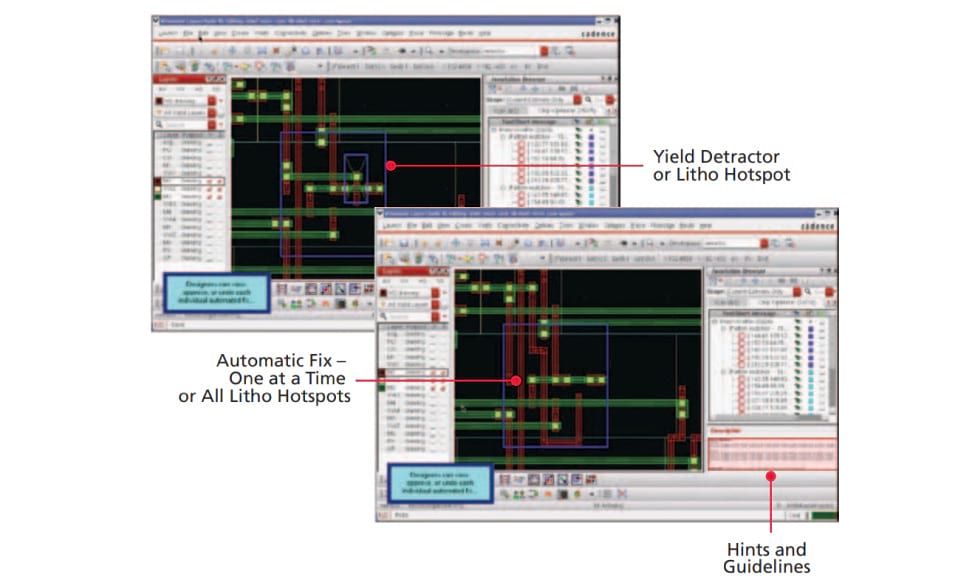
Virtuoso DFM enables in-design DRC+, an innovative DFM approach launched by GLOBALFOUNDRIES for 28nm. Cadence has been an early development partner with GLOBALFOUNDRIES in the development of DRC+ flow, which leverages Cadence pattern-classification technology to classify yield detractors into pattern families, and Cadence pattern-matching technology to find the yield detractors on designs. Designers can use their own yield-detractor pattern library or foundrycertified pattern library to use fast, production-proven 2D pattern matching to search the design for potential yield detractors. With just a few clicks in the GUI, designers can perform automatic fixing for each error at a time or all in one shot, with an automated recheck to ensure no new hotspots were created. The targeted application of relaxed DRCs at identified critical locations improves printability and yield without sacrificing design area.
Virtuoso DFM also enables in-design litho hotspot detection and correction. The built-in foundry-golden Litho Physical Analyzer delivers model-based litho hotspot analysis fast enough to let designers uncover yield critical hotspots during custom-design implementation. Again, with a few clicks in the GUI designers can perform real-time automatic fixing for each hotspot or all hotspots in one shot with an automated recheck to ensure no new hotspots were created.
In-design, constraint-driven, layoutdependent-effects variability analysis and optimization
At advanced nodes, a leading cause of systematic variability is the application of mechanical stress to transistors. Stress is commonly used to enhance performance in CMOS ICs, but it also causes layoutdependent variability that can make it difficult to close timing. The variability of stress is the problem—not the stress itself. But stress is also unintentionally induced through various technologies such as shallow trench isolation (STI), a widely used technique that uses oxide to isolate transistors. The well proximity effect (WPE) results from the location of well boundaries with respect to transistors. WPE is not a stress effect, but it does impact mobility and threshold voltage, and it is a proximity effect that impacts the stress liner. These effects and others constitute what is known as LDE variability.
Evaluating LDE variability is not straightforward, because the evaluation must consider “proximity effects.” This means that designers can’t just look at transistors in isolation. The location and dimensions of neighboring layout features change the surrounding stress, creating mismatches between the layout and the schematic—resulting in long iteration loops and delayed time to market. These loops can be painstakingly long for an analog designer as they go from completed layout to extract stress parameters, and then run full simulation to complete a loop.
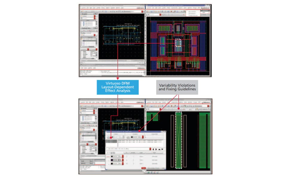
Virtuoso DFM integrates silicon-accurate, layout-dependent-effect electrical analyzer technology to deliver in-design LDE analysis and optimization. With Virtuoso DFM, designers can perform layout-dependent-effect electrical analysis during the creation of the layout, without requiring a complete layout and full simulation information. Virtuoso DFM performs a static check on the transistor layout to quantify the impact of layoutdependent effects on transistor current, and then excessive variations are flagged and reported to the layout designer for layout optimization.
Virtuoso DFM also supports designer’s constraint-driven, layout-dependenteffect variability analysis. Designers verify that the layout meets intended matching constraints while layout is being constructed, and provide guidelines to drive layout modifications to mitigate the layout dependent effects.
Comprehensive foundry support
Cadence signoff DFM technologies are certified by leading foundries and are also the internal tool of choice at multiple foundries. Cadence pattern matching analysis is the golden internal pattern matching engine to support the leading 28nm DRC+ flow. Cadence Litho Physical Analyzer is the golden engine at major foundries and their customers to systematically detect hotspots on designs prior to manufacturing. Layout-dependenteffect electrical analyzer has proven to deliver silicon accurate variability analysis and is used by leading foundries and IDMs to characterize their libraries for stressproximity effects.
Specifications
Foundry support
- Certified and supported by leading foundries and IDMs
- Flow-tested and qualified with foundry DFM design kits (DDKs) and yielddetractor libraries
Platforms
- Linux (32-bit, 64-bit)