- Overview
- Key Features and Benefits
- Design Planning and Implementation with System Planner and Innovus Implementation
- Integrity 3D-IC Database
- Co-Design of Digital Chiplets with Analog/RF and Packaging
- Native 3D Implementation Flows
- Specialty Routing for Silicon Interposers
- Flow Manager for Early Analysis Flows
- Cadence Services and Support
Datasheet
Integrity 3D-IC Platform
System-driven PPA closure for 3D-IC designs
A slowdown in Moore’s Law and the rising costs of advanced nodes is driving advanced packaging, leading to chip stacking with silicon substrates for a variety of applications. New 3D implementation and system planning challenges emerge as chip stacking creates new complexities related to different components of the stack and the system as a whole, with extra considerations to be given to mechanical, electrical, and thermal aspects of the whole stacked system. To have an efficient working 3D-IC stack, it is important to look at systemlevel planning and implementation with closed-loop embedded system-level analysis. The Cadence Integrity 3D-IC Platform provides an industry-first holistic and comprehensive 3D-IC design planning, implementation, and analysis platform to take the full system view and perform system-driven optimization of performance, power, and area (PPA) for chiplets and co-design of interposers, packages, and printed circuit boards for 3D-IC applications.
Overview
Overview
The high-capacity Integrity 3D-IC design and analysis platform (Figure 1), built on the infrastructure of Cadence’s leading Innovus Implementation System, helps systemlevel designers plan, implement, and analyze any type of stacked die system with a variety of packaging styles (2.5D or 3D). Providing industry’s first integrated comprehensive system and SoC-level solution that enables system analysis technology along with co-design with Cadence’s Virtuoso and Allegro analog and package implementation environments.
Integrity 3D-IC provides an integrated flow manager for setup of system-level analysis capabilities for thermal analysis, power analysis, inter-die static timing analysis, and physical verification early in the loop to achieve efficient closure at not just the individual die level but on the system as a whole.
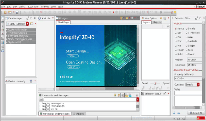
Figure 1: Integrity 3D-IC Platform
Key Features and Benefits
-
 New single-cockpit, high-capacity 3D design planning and implementation platform for handling all types of 3D-IC stacks enabled by foundries
 - Powerful cross-platform co-design capabilities with the Virtuoso and Allegro environments
- Elegant flow manager to set up early power-thermal analysis, cross-die static timing analysis, and inter-die physical verification
- Unique hierarchical planning and optimization capabilities for system-level design through the system planner
- Complete stack management, chip-to-package signal mapping, and advanced bump and TSV planning through realtime TCL-based direct integration with Innovus Implementation
- Powerful 2D to 3D exploration flows for homogenous stacked die exploration with memory-on-logic and logic-on-logic exploration
- Efficient on-disk database for hierarchical multi-level representation of each tier
Design Planning and Implementation with System Planner and Innovus Implementation
The Integrity 3D-IC platform’s system planner helps designers to set up and integrate all the stacking devices of a 3D design, including digital dies, analog dies, packages, and PCB boards. Compared to the layout view’s massive design data, the system planner provides a lightweight view of the 3D-IC system, focusing on the die-to-die stacking configuration, floorplanning, die-to-die interface design, and optimization. The layout implementation works on a full Innovus database and provides all the placement, routing, and optimization capability that a digital IC designer needs. It provides 3D partitioning features needed for designing a digital die or interposer of the 3D system.
In addition, Integrity 3D-IC also provides a multi-die layout view, so that designers can check multiple dies with different process nodes in a single GUI and then display the system analysis result for debugging and locating cross-die design problems. Integrity 3D-IC gives designers the flexibility to switch between the system planner and layout implementation seamlessly (Figure 2). Design data can be pushed to or pulled from the planner as die floorplan, bumps, TSVs, I/O pads, and hard macros are changed so that they are always synced across all the stacking devices.
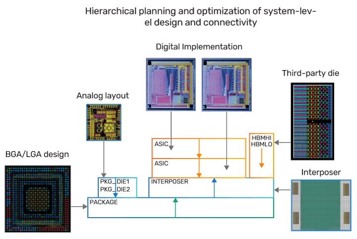
Figure 2: Hierarchical planning and optimization of system-level design and connectivity
Integrity 3D-IC Database
At the center of the development of Integrity 3D-IC is a common hierarchical multi-technology database that connects the system, package, and substrate with multiple tiers of the ICs. The database can support reading multiple technology files belonging to different technology nodes. The design data of each 3D-IC device is saved and organized under this single database directory. The database’s native Tcl commands make it easy to read, write, update, display, and overlay design databases and analysis results. As a natural extension of Innovus Implementation’s hierarchical database, the Integrity 3D-IC database (Figure 3) also supports a digital die that itself is a hierarchical design.
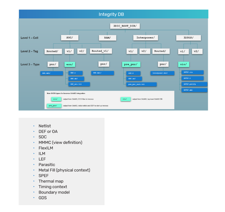
Figure 3: Integrity 3D-IC design database elements
Co-Design of Digital Chiplets with Analog/RF and Packaging
For analog or RF designs, the primary platform for implementation is the Virtuoso environment. Integrity 3D-IC interfaces with the Virtuoso environment through the system planner. A design completed in the Virtuoso environment can have the data from the bumps passed and read to the other die in the Integrity 3D-IC platform to create optimal location for the connecting bumps on the second die. Cadence supports the OpenAccess database, which provides a natively unified database for interoperation between the Innovus and Virtuoso platforms. The already existing data exchange capability through OpenAccess is further leveraged to exchange design data between Virtuoso and Integrity 3D-IC environments.
IC packaging is a critical link in the silicon-package-board design flow. The Allegro environment offers complete and scalable technology for the design and implementation of PCBs and complex packages. Cadence’s IC package design technology allows designers to optimize complex, single-, and multi-die wire bond and flip-chip designs for cost and performance, while meeting short project timelines. An IC package database from the Allegro environment can be directly imported into the Integrity 3D-IC platform for bump connections with interposers and substrates. This enables package co-design while considering the whole system in a single environment, making the package design step significantly simpler.
Native 3D Implementation Flows
Integrity 3D-IC offers a range of native 3D stacking sub-flows. By disintegrating the 2D netlist into a multi-tier 3D stack, users have added capability to explore the PPA benefits of a 3D stacked die system over a planar 2D single die design.
Due to the well-known “memory wall” limitations of Moore’s law—where the size and speed of on-chip memories are not able to catch up with the rate of increase of the number of transistors in a processor design—a memory die mounted on top of a logic die is a popular 3D stacking style for improving memory latency. Integrity 3D-IC leverages a unique mixed placement technology from Innovus Implementation to separate out the memory macros from a 2D design and automatically partition and implement it into two homogenous tiers with a memory die on top and a logic die with standard cell logic on the bottom tier (Figure 4). Since some logic, such as test logic, may need to reside on the same die as the memories, the flow also supports user control by selectively assigning macros and logic partition to different tiers. The flow relies on 3D mixed placement , shadow bump assignment, and a physical unfolding of the design to achieve a fully placed timing-aware stacked design. Once that’s accomplished, the user can continue to run standard implementation steps like CTS, optimization, routing, and post-route steps as normal place and route flows to finish 3D implementation.
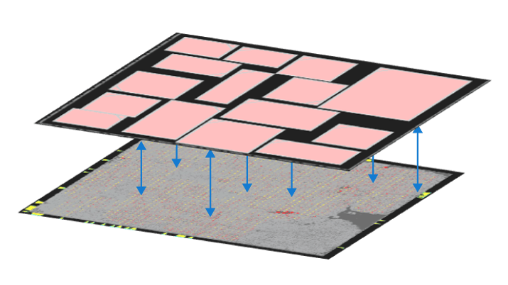
Figure 4: Homogenous 3D stack for memory-on-logic flow
Specialty Routing for Silicon Interposers
Cadence’s NanoRoute Advanced Digital Router is the industry-leading unified routing and interconnect optimization solution that helps you quickly achieve concurrent timing, area, signal integrity, and manufacturability convergence during digital implementation (Figure 5). The NanoRoute tool handles all routing challenges at both block and full-chip levels, by combining the performance characteristics of a grid-based router with off-grid flexibility, and it simultaneously evaluates and optimizes interconnect topology based on the 3D effects on timing, area, power, manufacturability, and yield enabling implementation of high-performance designs on advanced or mainstream process technologies.
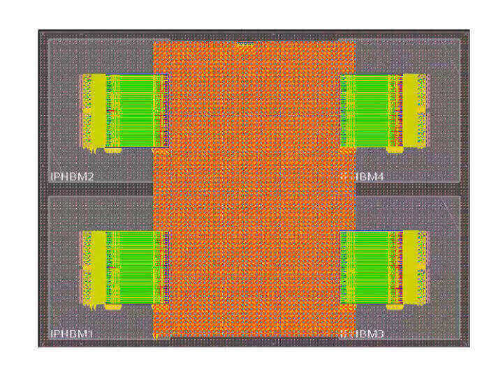
Figure 5: Chip-level digital implementation examples
This ensures a smooth path to design tapeout and production silicon while simultaneously evaluating and optimizing the interdependent objectives of signal integrity, manufacturing awareness, routing, and timing for faster design convergence—all while preserving design intent.
The auto-routing solution enables a fully automated interposer routing to connect macro bumps with bus routing patterns using special commands. Benefits of the auto-routing solution include:
- Close to 100% high shielding ratio
- Very fast run time (in minutes)
- Evenly distributed wirelength
- Minimal via count
Flow Manager for Early Analysis Flows
While building a 3D system, early signoff analysis is key to get system-level feedback and make design changes during architecture selection. In addition to standard analyses such as static timing and power, electromigration, IR analysis, and physical verification, stacked die system requires additional signoff checks, including thermal analysis and mechanical stress analysis for warpage. Integrity 3D-IC offers a flow manager that guides the user through different analysis setups relevant to the third dimension. After the system floorplanning is complete and the design is implemented, a list of analyses (Figure 6) is available in the flow manager.
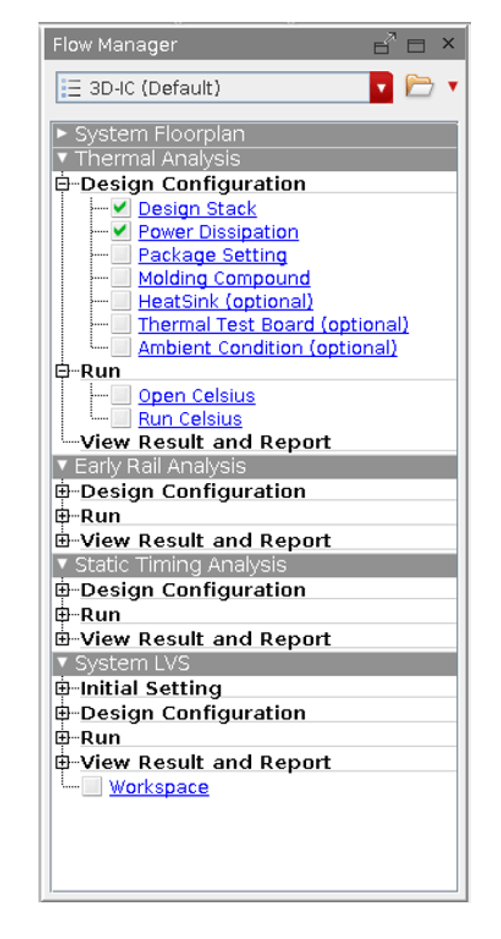
Figure 6: Flow manager
Thermal Analysis Flow Through Celsius Thermal Solver
The performance of 3D-IC designs is dependent on the thermal behavior and temperature distribution among components of the 3D-IC system. The Cadence Celsius Thermal Solver environment enables all aspects of thermal analysis to quickly and accurately identify thermal problems in IC packages and PCBs, including stacked die systems (Figure 7). It includes a powerful finite element analysis (FEA) field solver to analyze both transient and steady-state and heat conduction in complicated solid structures and utilizes a computational fluid dynamics (CFD) engine for convection and radiation heat transfer analysis. The 3D FEA field solver provides accurate thermal conduction analysis and electrical simulation for arbitrary 3D structures, such as complicated packages with bumps or bonding wires, connectors, and transitions of connectors to the PCB.
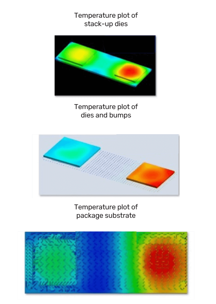
Figure 7: Thermal analysis examples
Early Rail Analysis Using Voltus Solution
Power delivery network that carries current to each die and across to other dies is one of the most important aspts of 3D-IC. The performance of 3D-IC designs is heavily dependent on the power allocation/distribution and IR drop effects among multiple dies. Integrity 3D-IC, with its ability to perform early rail analysis (ERA) of 3D-IC designs, provides multi-die stack-up data with detailed designs and optimized connections (Figure 8). It uses capabilities from the Cadence Voltus IC Power Integrity Solution, a standalone, cloud-ready, full-chip, cell-level power signoff tool that provides accurate, fast, and high-capacity analysis and optimization technologies on a power delivery network (PDN) or the power grid of a chip. It is well integrated with Cadence’s Sigrity XtractIM and Sigrity PowerDC technologies for chip-package-board total power signoff co-analysis, including 2.5D silicon-interposer and 3D-IC technologies.
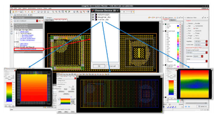
Figure 8: Power allocation and distribution design
Multi-Die STA Flow Through Tempus Solution
With multiple chiplets , it is important to close timing individually on each die and time any synchronous paths that go across dies. Direct die stacking shortens interconnects but adds to the complexity of modeling 3D stacking structires like through silicon vias and microbumps. Cadence’s Quantus Extraction Solution is updated to model all the 3D structures and create multiple SPEFs using standard ICT techfiles and inter-process technology files. Once the individual spec files are extracted, the Cadence Tempus Timing Signoff Solution provides fast multi-die static timing analysis (STA) capabilities with unique distributed processing and cloud capabilities (Figure 9). The Tempus solution has the ability to use boundary model abstracts for on-die interfaces and ability to natively perform delay calculation for inter-die interconnects. In addition, various process RC corners must be considered for stacked die designs, ensuring the complete coverage of process variation for accurate timing analysis. The Tempus solution uses special techniques for die-to-die path analysis and smart corner pruning to reduce signoff corners. The minimized design database and reduced corner complexities provide accurate analysis result without sacrificing design performance and expedite design timing closure.
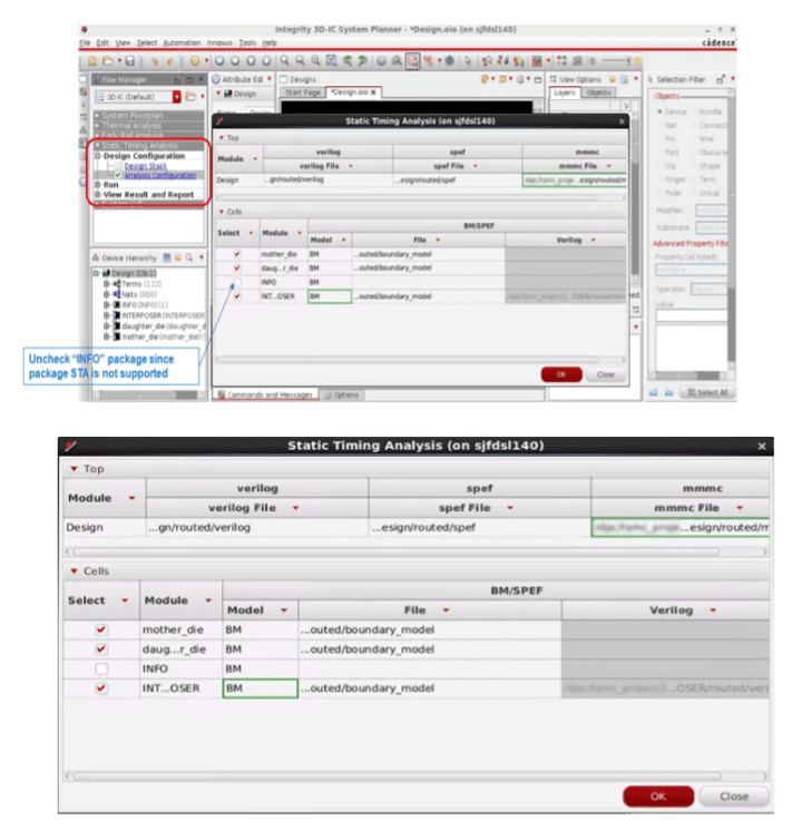
Figure 9: Static timing analysis
Inter-Die Connectivity and DRC Checking Using Pegasus Physical Verification
In a multi-chiplet system with stacked dies or on an interposer, there are critical inter-die connectivity and design rule checks (DRCs) that are mandatory for design closure. Integrity 3D-IC incorporates the Cadence Pegasus Physical Verification System’s flexible cloud-ready platform that enables rule-deck free multi-chiplet connectivity physical verification at the system level (Figure 10).
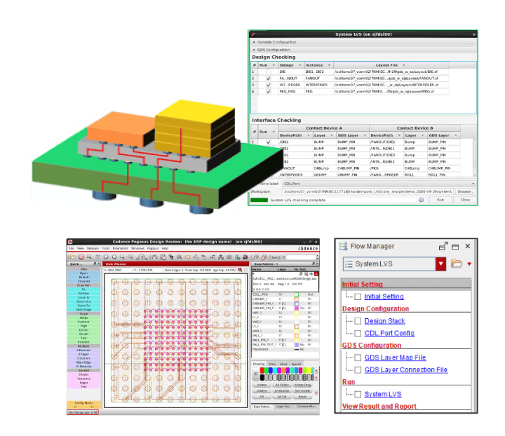
Figure 10: Physical verification example
Pegasus Physical Verification can check bump alignment and system-level connectivity using self-generated data through a GUI-driven interface and is embedded with an interactive GDS viewer. The native integration between Integrity 3D-IC and Pegasus Physical Verification ensures accurate physical verification with no third-party requirement in the 3D design flow.