Key Benefits
- Team-based constraint-driven design flow: PCB layout specialists perform first-order PI analysis so the PI expert can focus on advanced analysis tasks
- Automate the AC and DC PI analysis set-up, and reuse previous set-ups to allow design changes to be quickly and easily analyzed
- Easily identify layout and routing changes necessary to meet PDN-specific requirements with DRC markers and cross-probing
In PCB design, DC analysis is vital as numerous factors combine to exacerbate the problem of power integrity. Core voltage levels continue to drop; 1.2V and less are now common. As voltage is reduced, current requirements typically increase (IR drop = I * R). The miniaturization of electronics results in fewer layers and higher densities, thus reducing the available area for power nets. And antipads around vias perforate the planes and can overlap, creating the “Swiss cheese” effect.
In addition, there are the power delivery network (PDN) challenges for a PCB designer, starting with the multiple instructions from hardware designer or power integrity (PI) engineer that are communicated by email, phone call, rules of thumb, etc. The designer must apply all of those instructions and rules to multiple power supplies. Having done that, the designer must then attempt to fulfill additional requests, such as “Can you shrink it by 20%?”, “Can you remove two plane layers and five capacitors?”, and that age-old favorite, “Can you do it yesterday?”
Complex boards can have dozens of power rails, hundreds of power nets (including filter nets) and even more components that make up the PDN. Sorting through hundreds of pages of schematics to ensure that the PDN is logically connected is one pain point. However, it may become even more painful on the back-end of the design process when power integrity analysis requires that all those nets and components be specified and modeled for power integrity analysis. This may take days or even weeks just to setup.
An additional challenge is how the design issues are communicated: How does the PI engineer communicate issues and guidance to the PCB designer? How does the PCB designer communicate solutions to the PI engineer? How can the PCB designer determine if a solution is good? Fortunately, integration features are available to assist the PCB designer and PI engineer with these design and communication issues. In addition, the PCB designer has tools available to him to automatically calculate first-order electrical constraints to help get started if the PI engineer has not yet communicated the guidance.
PowerTree Graphical Environment
The Cadence Allegro® PowerTree™ technology allows the PCB layout specialists and hardware designers to graphically view source/sink definitions, discrete values, model names, net names, decoupling capacitor values, target impedance constraints, and more in the logical PDN topology.
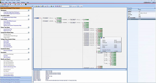
Hardware designers can perform early analysis sanity checks at the push of a button. By using schematic data, they can determine if the PDN topology has been properly captured to meet the design criteria.
By empowering hardware designers and PCB layout specialists to perform simple analysis, PI experts can focus on more specialized analysis. With automated setup from PowerTree technology, PI experts and non-experts alike no longer need to spend days or weeks setting up PI analysis. Applying the PowerTree data to the physical design makes simulation as easy as the click of a button.
Integration Features
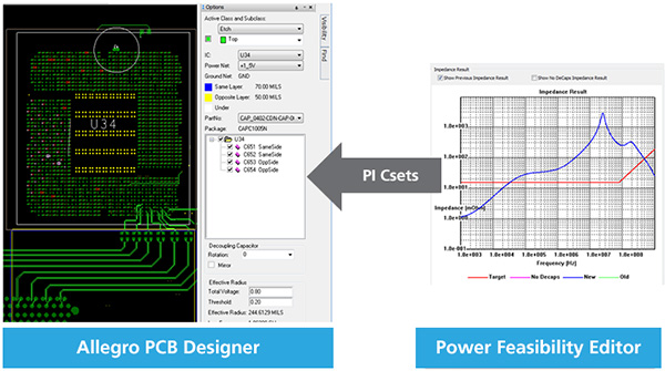
Decoupling capacitor placement rules require the PI expert to perform analysis to determine the ideal de-cap scheme for each IC. In addition, PI expert must creates PI constraint sets to guide the PCB designers decap placement.
DRC markers determined by PI designers’ rules are annotated to the Cadence Allegro PCB Designer. These markers enable the PCB designer to understand PDN issues discovered by the PI engineer and address them.
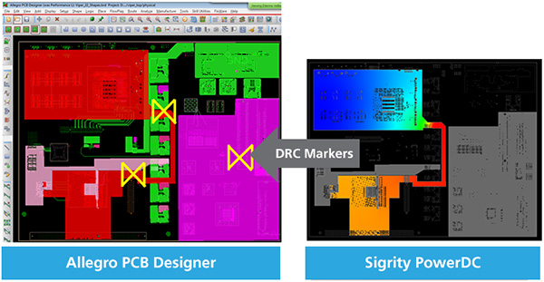
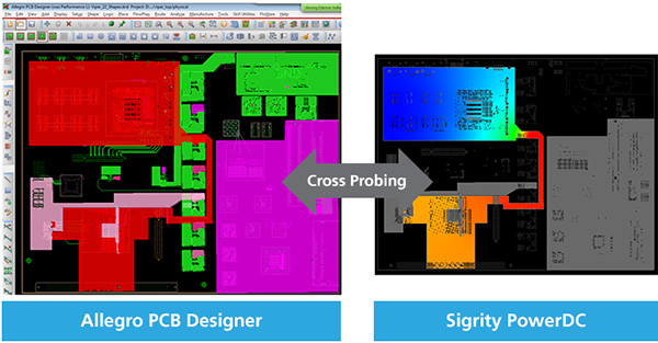
Cross-probing between Allegro PCB Designer and analysis results enables the PCB designer to use the visual analysis results to determine what needs to be changed in the PCB, such as increasing the size of power shapes, adding vias, adding planes, etc.
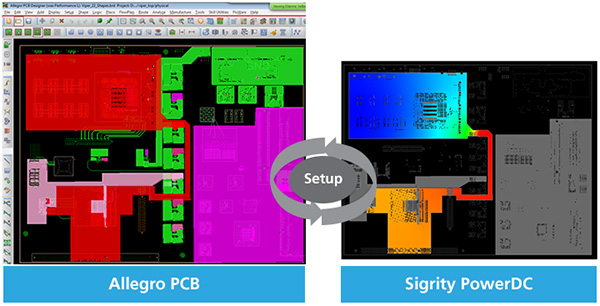
Re-using the PI expert's set-up enables the PCB designer to change and re-analyze the design, including the changes to the original set-up.
Allegro/Sigrity Integration
Allegro Sigrity™ PI Base integrates Allegro and Sigrity technology for PI analysis of PCB, IC package, and system-in-package (SiP) designs, and enables constraint-driven design with an integrated layout and analysis solution. The Allegro Sigrity PI Base’s primary advantages include:
- Proven Sigrity analysis engines
- Automated set-up using PowerTree data captured from the schematic
- Industry’s first constraint-driven PI design process to drive decap selection and placement
- Automated cross-probing configuration after DC analysis to easily identify and resolve IR drop issues in physical layout
- Targeted for layout designers and PI engineers
- Add-on options for detailed analysis, compliance, and assessment


Training and Support
Need Help?
Training
The Training Learning Maps help you get a comprehensive visual overview of learning opportunities.
Training News - Subscribe
Online Support
The Cadence Online Support (COS) system fields our entire library of accessible materials for self-study and step-by-step instruction.
Request SupportTechnical Forums
Find community on the technical forums to discuss and elaborate on your design ideas.