Datasheet
Cadence First Encounter Design Exploration and Prototyping
A flexible, signoff-driven environment for fast implementation of giga-scale designs
Cadence First Encounter Design Exploration and Prototyping offers a comprehensive flat and hierarchical design planning, analysis, and debug environment for complex designs. Its GigaFlex technology adapts to growing capacity requirements while still retaining the relevant timing, placement, and congestion information to accurately plan and implement 100M+ instance designs. The latest advanced node and low-power capabilities make hierarchical implementation of high-speed and advanced node designs faster and easier, and produce designs that consume lower power. In addition, with unique partitioning and budgeting capabilities, First Encounter technology ensures convergence and provides a predictable path to design closure.
Overview
First Encounter Technology
Accommodating today’s chip design requirements within narrow market windows has led to a predictability crisis. How can engineers determine design feasibility for larger, higherperformance, power-hungry chips with an incomplete netlist, library, and constraints? And how can they quickly assess floorplans for congestion, timing, and power without having to go into real implementation?
First Encounter technology addresses these challenges and more. It spans silicon virtual prototyping, automatic floorplanning, physical synthesis, hierarchical controls for partitioning and budgeting, legal macro and standard cell placement, complete power-grid design and optimization, and hierarchical clock synthesis for high-performance, complex 100M+ instance designs. With such comprehensive capabilities, First Encounter technology helps customers meet their time-to-market requirements confidently, and with significant performance and productivity gains.
Benefits
Predictability and convergence
-
 Enables early design exploration and accurate chip feasibility analysis
 - Performs automated floorplan synthesis and ranking for a flexible, predictable path to design closure
Productivity and faster time to market
- FlexModels and FlexILM abstraction technology adapts to the flow, providing the right mix of capacity and accuracy, enabling designers to achieve up to 20x improvements in capacity and turnaround time
- Partition-in-partition technology natively manages multi-level hierarchical designs
- Supports hierarchical methodologies such as bottom-up block-based flows, top-down black-box flows, and hybrid flows for 100M+ instance designs
- Provides a unified flow for partitioning, pin assignment, macro placement, feed-through insertion, pipeline registers, clock planning, and time budgeting
- Delivers intuitive and visual global timing, power, and clock debug and diagnostics features
Ease of use
- Integrates design flows and common engines from the front-end, implementation, and packaging domains
- Delivers a ready-to-use prototyping foundation flow with design exploration to get to an implementation-ready floorplan
Product differentiation and lower cost
- Supports concurrent chip/package design and optimization
- Supports integrated automatic area and peripheral I/O placement and optimization
- Supports flip-chip RDL routing capabilities
Features
Early design exploration
Today’s physical design teams start physical implementation and design planning very early in the design cycle— with multiple versions of the design netlist—to determine design feasibility. Among their questions: Can the design be implemented in the required area? Can the design operate at the desired speed? Does it meet power requirements?
First Encounter technology addresses all of these issues and more:
- Production-proven automated floorplan synthesis closes the gap between architecture and implementation by enabling timing-, power-, area-, and congestion-aware placement coupled with fast global routing and in-place optimization
- Concurrent standard cell and macro placement helps designers generate implementation-quality floorplans for both flat and hierarchical designs
- Built-in flexibility and editing capabilities such as Relative Floorplan (specifying relationships for pre-routes, resizable objects, multiple relations, datapath stacking, and integrated analysis tools) and Resize Floorplan enable you to quickly and accurately reach an optimal final floorplan
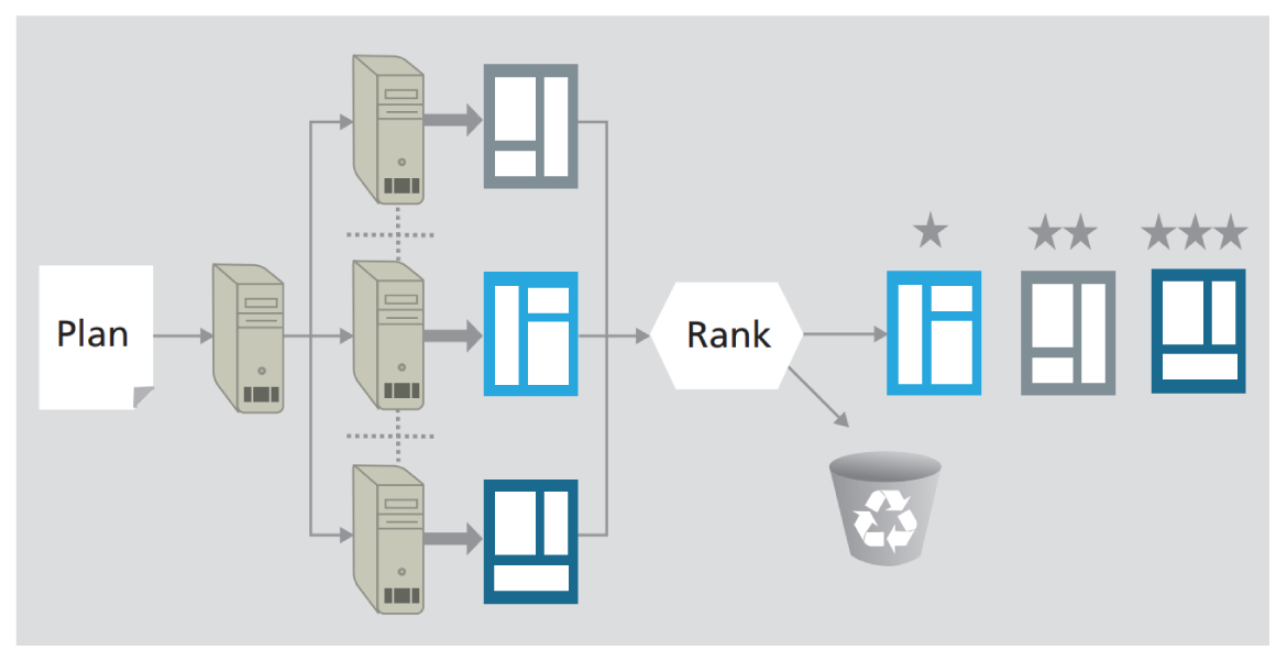
- The floorplan ranking system automatically generates multiple floorplan scenarios in parallel and analyzes them based on pre-defined quality-of-results criteria; you can explore as much of the physical solution space as possible and make the most informed tradeoffs for design feasibility
- GigaFlex abstraction modeling enables very early and fast design planning for giga-scale designs; it allows netlist compression up to 90% while maintaining relevant timing and congestion information, resulting in faster turnaround time and one-pass implementation handoff
To bring physical predictability into your estimations, you can link into the First Encounter environment from the Cadence Chip Planning System.
Silicon virtual prototyping and hierarchical capabilities
First Encounter technology supports all implementation styles—from flat or hierarchical to single or multi-VDD. Capabilities for fast power-grid design and optimization, global routing, in-place optimization, and global timing debug provide a robust infrastructure to implement any methodology.
- Full-chip flat prototyping delivers complete physical, timing, clock, and power data, thereby eliminating the guesswork associated with traditional block-based approaches
- Hierarchical support helps physical designers assess how best to partition the logical hierarchy into physical modules by analyzing the optimal pin assignments; enabling quick time budgeting; accurately predicting the clock distribution networks; analyzing the power grids; and eventually generating complete timing and physical constraints for each of the physical modules
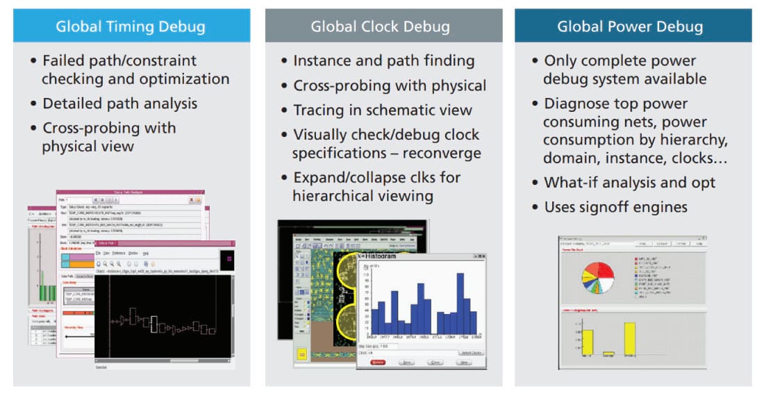
Fast and easy debug and analysis
The ability to debug and diagnose interdependent design closure issues is critical. The challenges often come late in the design cycle, along the critical path to final tapeout. First Encounter capabilities for timing, power, and clock debug and diagnostics enable you to quickly pinpoint and visualize interdependent timing, clock, and power issues, and then quickly resolve them using powerful “what-if” analysis techniques. You can implement the results immediately in the physical design.
Low-power design
Advanced low-power design techniques such as power gating (MTCMOS) and dynamic voltage and frequency scaling (DVFS) use multiple power domains. The underlying First Encounter infrastructure facilitates the implementation of low-power designs because it comprehends multiple power domain structures across the flow. This capability enables automatic placement of level shifters, with all power connections completed automatically. First Encounter technology also supports Common Power Format (CPF) and IEEE 1801 to specify advanced power-reduction techniques, from design and verification through final implementation and signoff.
Concurrent chip/package design and flip-chip support
First Encounter flip-chip floorplanning technology enables the concurrent design of chip and package by including package constraints and parasitic effects while designing the IC. With support for multiple I/O methodologies, concurrent optimization of I/O and core instances, automatic RDL routing (including 45-degree support), and accounting for RDL routing during signal/power routing, First Encounter flip-chip technology eliminates the manual steps in I/O placement and optimization. This mature technology has been proven through multiple customer tapeouts.
Platforms
- lnx86: Linux (x86 and x86_64) 32/64-bit
- sol86: Solaris (x86_64) 64-bit
- sun4v: Solaris (ultraSparc) 64-bit
- ibmrs: AIX (power) 64-bit