Datasheet
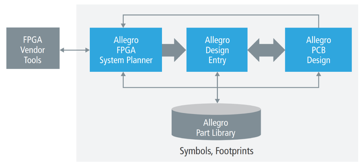
Allegro FPGA System Planner
FPGA-PCB co-design with automatic rules-driven pin assignment
The Cadence Allegro FPGA System Planner addresses the challenges that engineers encounter when designing one or more large-pin-count FPGAs on the PCB board—which includes creating the initial pin assignment, integrating with the schematic, and ensuring that the device is routable on the board. It delivers a complete, scalable technology for FPGA-PCB co-design that automates creation of optimum “device-rules-accurate” pin assignment. By replacing manual, error-prone processes with automatic pin assignment synthesis, this unique placement-aware solution eliminates physical design iterations while speeding optimum pin assignment.
Cadence FPGA System Planner technologies are available as:
-
 Allegro 2 FPGA System Planner Option
 - Allegro 4 FPGA System Planner Option
- Allegro ASIC Prototyping Option
- OrCAD FPGA System Planner
Overview
Designing Large-Pin-Count FPGAs on PCBs
Integrating today’s FPGAs—with their many different types of assignment rules and user-configurable pins— on PCBs is time consuming and extends design cycles. Often the pin assignment for these FPGAs is performed manually at a pin-bypin level in an environment that is unaware of the placement of critical PCB components that are connected to FPGAs. Without understanding the impact to PCB routing, FPGA-based design projects are forced to choose between two poor options: live with suboptimal pin assignment, which can increase the number of layers on a PCB design; or deal with several unnecessary iterations at the tail end of the design cycle. Even with several iterations, this manual and error-prone approach can result in unnecessary PCB design re-spins.
With the added time required to generate pin assignments for FPGAs using manual approaches, users are unable to do tradeoffs between the different FPGA devices available and the cost of devices used in an FPGA sub-system. This is because performing the tradeoffs would mean that users would have to do two projects in parallel with no design reuse of any kind between the two.
Allegro FPGA System Planner
The Allegro FPGA System Planner provides a complete, scalable solution for FPGA-PCB co-design that allows users to create an optimum correctby-construction pin assignment. FPGA pin assignment is synthesized automatically based on userspecified, interface-based connectivity (design intent), as well as FPGA pin assignment rules (FPGA rules), and actual placement of FPGAs on PCB (relative placement). With automatic pin assignment synthesis, users avoid manual error-prone processes while shortening the time to create initial pin assignment that accounts for FPGA placement on the PCB (placement-aware pin assignment synthesis). This unique placementaware pin-assignment approach eliminates unnecessary physical design iterations that are inherent in manual approaches.
With a way to quickly synthesize optimum pin assignment using userspecified design intent at a high level, the Allegro FPGA System Planner enables designers to explore their FPGA-based architecture and to create an optimum correct-by-construction pin assignment for either production or prototype designs that use FPGAs.
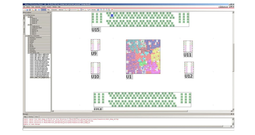
The Allegro FPGA System Planner is integrated with the Cadence design creation tools: Cadence OrCAD Capture and Cadence Allegro Design Entry (CIS and HDL). It reads and creates schematic symbols for both OrCAD Capture and Allegro Design Entry HDL. In addition, a floorplan view uses existing footprint libraries for OrCAD PCB Designer and Allegro PCB Editor. Should placement change during layout, pin optimization using the Allegro FPGA System Planner can be accessed directly from the Allegro PCB Editor.
Benefits
- Scalable, cost-effective FPGA-PCB co-design solution from OrCAD to Allegro tools
- Accelerates integration of FPGAs with OrCAD Capture and Allegro Design Authoring solutions
- Shortens time for optimum initial pin assignment, accelerating PCB design schedules
- Eliminates unnecessary, frustrating design iterations during the PCB layout process
- Eliminates unnecessary physical prototype iterations due to FPGA pin assignment errors
- Reduces PCB layer count through placement-aware pin assignment and optimization
- Planning mode allows PCB designers to propose FPGA pin (re)assignments based on route planning, reducing number of layers or time to route designs or both
Features
Allegro FPGA system planner technology
An FPGA system is defined as a subset of the PCB design that includes one or more FPGA and non-FPGA components that are connected to FPGAs.
Traditional approaches to pin assignment are typically manual and often based on a spreadsheet. Tools such as these require users to do pin assignment without taking into consideration the placement of other components and routability of the interfaces and signals. Above all, there is no online rules-checking to ensure that the right pin types are being used for the signals that are assigned to the FPGA pins. As a result, users have to make several iterations between the spreadsheet-based tools and the tools from FPGA vendors. Often this adds an increased number of iterations between the PCB layout designer who cannot route the signals from FPGA pins on available layers and the FPGA designer who has to accept paper-based or verbal pin-assignment suggestions from the PCB layout designer. Once a change is made to the pin assignment by the FPGA designer, the pin assignment change has to be made in the schematic design by the hardware designer. Such iterations add several days if not weeks to the design cycle and possibly a great deal of frustration for the team members. Since this is a manual process, mistakes that are not detected can also cause expensive physical prototype iterations.
While it may help to automate the synchronization of changes made to the pin assignment by the FPGA designer, hardware designer, or PCB layout designer, it doesn’t reduce the root cause of these iterations. Pin assignment that is not guided by all three aspects—FPGA resource availability, FPGA vendor pin assignment rules, and routability of FPGA pins on a PCB—requires many iterations at the tail end of the design process, thereby extending the time it takes to integrate today’s complex, large-pincount FPGAs on a PCB.
Specifying design intent
The Allegro FPGA System Planner comes with an FPGA device library to help with selection of devices to be placed. It uses OrCAD PCB Designer or Allegro PCB Editor footprints for the floorplan view and allows users to quickly create relative placement of the FPGA system components.
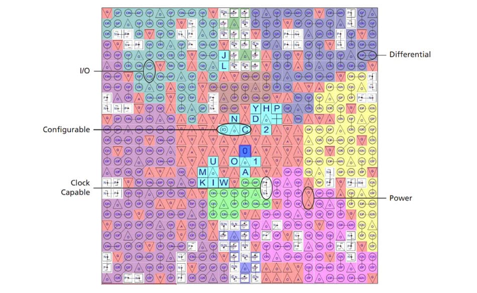
The Allegro FPGA System Planner allows users to specify connectivity between components within the FPGA sub-system at a higher level through interface definitions. Users can create interfaces such as DDR2, DDR3, and PCI Express, and use these to specify connectivity between a FPGA and a memory DIMM module or between two FPGAs. The Allegro FPGA System Planner understands differential signals, and power signals, as well as clock signals.
FPGA device rules
The Allegro FPGA System Planner comes with a library of device-accurate FPGA models that incorporate pin assignment rules and electrical rules specified by FPGA device vendors. These FPGA models are used by the synthesis engine to ensure that the vendor-defined electrical usage rules of the FPGAs are strictly adhered to. These rules dictate such things as clock and clock region selection, bank allocation, SSO budgeting, buffer driver utilization, I/O standard voltage reference levels, etc. During synthesis, the Allegro FPGA System Planner automatically checks hundreds of combinations of these rules to ensure that the FPGA pins are optimally and accurately utilized.
Placement-aware PIN assignment synthesis
The Allegro FPGA System Planner provides users a way to create an FPGA system placement view using Allegro PCB footprints. Users specify connectivity between components in the placement view and the FPGA at a high level using interfaces such as DDRx, PCI Express, SATA, Front Side Bus, etc. that connect FPGAs and other components in the design, shortening the time to specify design intent for the FPGA system.
Once the connectivity of the FPGA to other components in the sub-system is defined, the Allegro FPGA System Planner then synthesizes the pin assignment based on the user’s design intent, available FPGA resources, component placement around the FPGA, and the FPGA vendor’s pin assignment rules.
The Allegro FPGA System Planner has a built-in DRC engine that incorporates the rules provided by FPGA vendors for pin assignment, reference voltages, and terminations. This rules-based engine prevents PCB physical prototype iterations as the FPGAs are always correctly connected.
Pin assignment algorithms are optimized to assign interface signals to a group of pins, thereby minimizing net crossovers and improving routability on the PCB.
Architectural exploration enabled
During the device selection process, FPGA designers need a way to evaluate if the FPGA(s) they choose can meet their application needs while keeping the cost of devices as low as possible. Estimating FPGA resource requirements can be tricky and requires designers to balance look-up tables (LUTs), high-speed I/O requirements, and memory with I/Os for low-speed signals. Sometimes choosing more than one FPGA may be cheaper than choosing one large FPGA. While at other times, choosing an FPGA with a larger pin count will suffice, thereby saving board space and routing channels.
Manual pin assignment approaches make performing these cost and performance tradeoffs very time consuming and tedious. With its placement-aware FPGA I/O pin assignment synthesis, the Allegro FPGA System Planner helps designers do tradeoffs quickly, enabling architectural exploration that is not practical with manual approaches.
ASIC prototyping using FPGAs
Some companies choose to do ASIC prototyping using FPGAs on the PCB. In these cases, the number of FPGAs used grows rapidly. This sometimes requires using several PCBs to place all the FPGAs. With a large number of FPGAs, the time to do initial pin assignment can be very long using manual processes. Additionally, without taking placement of these FPGAs into account, the pin assignment can make routing of the PCB a very long process, extending the time it takes for designers to get to the ASIC prototype using FPGAs.
The Allegro FPGA System Planner shortens the time required to create pin assignment for a large number of FPGAs through placement-aware pin assignment synthesis that is driven by a device-accurate FPGA models library. With the ability to export port information in Verilog and import Verilog-based connectivity, the Allegro FPGA System Planner allows users to iterate with RTL partitioning software, shortening the time to define the FPGA-based system and quickly creating DRC-accurate FPGA pin assignment.
Tight integration with Cadence design creation
The Allegro FPGA System Planner generates Allegro Design Entry CIS and Allegro Design Entry HDL schematics for the FPGA sub-system. It uses existing symbols for FPGA in Allegro Design Entry symbol libraries. If the user desires, the Allegro FPGA System Planner can create split symbols for FPGA based on the connectivity or one split symbol per bank.
Integration with FPGA vendor tools
In addition to integration with Cadence PCB design tools, the Allegro FPGA System Planner communicates seamlessly with FPGA design tools. It generates and reads supported FPGA vendors’ pin-assignment constraint files. This capability enables the FPGA designer to evaluate pin assignments against the functional needs of the FPGA. Any changes made by the FPGA designer to account for these requirements can be imported into the Allegro FPGA System Planner so that the complete set of pin assignments remain in sync.
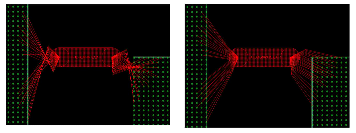
Optimizing FPGA pin assignments through Route Planning Mode
The initial pin assignment—that accounts for placement and routability of the FPGA on a PCB—goes a long way toward reducing costly design iterations between FPGA designer, PCB layout designer, and hardware designer. Once the PCB layout designer starts to plan the routing of interfaces and signals on FPGA, it is possible to further refine the FPGA pin assignment based on route intent, layer constraints, and fanout chosen for the FPGA.
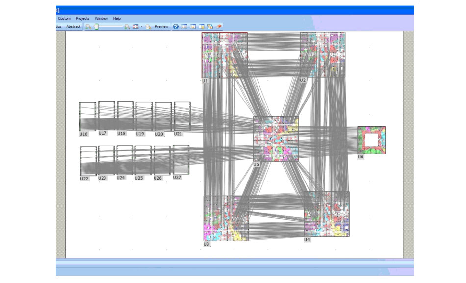
The Allegro FPGA System Planner allows users to optimize FPGA pin assignment during routing of the interfaces and signals on a FPGA by optimizing a set of signals tied to an interface based on the route approach. This optimization is performed by Allegro FPGA System Planner running as an engine under Allegro PCB Editor. Users have a choice of optimizing to the pin, to the break-out or completely reassigning the signals to a different bank. All of the pin reassignments are done in accordance with pin assignment rules provided by FPGA vendors. (See Figure 5)
Scalability
The Allegro FPGA System Planner technology is available in the following product offerings:
- Allegro ASIC Prototyping Option— For companies that use FPGAs to prototype ASICs for synthesizing and optimizing pin assignment of more than four FPGAs at a time
- Allegro 4 FPGA System Planner Option — For concurrent pin assignment, synthesis, and post-placement optimization of up to four FPGAs at a time, access to Route Planning Mode to allow PCB designers to propose pin reassignments based on route approach to FPGAs (see feature matrix for additional information)
- Allegro 2 FPGA System Planner Option —For pin assignment synthesis and post-placement optimization of a single FPGA
- OrCAD FPGA System Planner— For optimum initial pin assignment synthesis of a single FPGA
| Feature | DEMO | Allegro 2 FPGA System Planner Option | Allegro 4 FPGA System Planner Option | Allegro ASIC Prototyping Option |
|---|---|---|---|---|
| Max number of FPGAs in a design | No limit | 2 | 4 | No limit |
| Max number of pins with multiple FPGAs | No limit | 2,000 | 4,000 | No limit |
| Define connectivity at interface level | ✓ | ✓ | ✓ | ✓ |
| Automatic pin assignment based on rules, connectivity | ✓ | ✓ | ✓ | ✓ |
| Define JTAG chain manually | ✓ | ✓ | ✓ | ✓ |
| Define PROM chain manually | ✓ | ✓ | ✓ | ✓ |
| Forward annotation of component placement | ✓ | ✓ | ✓ | |
| Generate symbols and schematics | ✓ | ✓ | ✓ | |
| Export to PDF | ✓ | ✓ | ✓ | |
| Import constraints from Altera, Xilinx, and Actel | ✓ | ✓ | ✓ |
Operating System Support
Allegro platform technology
- Linux
- Windows
OrCAD technology
- Windows