White Paper
Impact of Finite Interconnect Impedance Including Spatial and Domain Comparison of PDN Characterization
Abstract
Over the past few decades, a lot of details have been worked out in power distribution network design, simulation and measurement. We have well-established PDN design procedures both in the frequency and time domains, we have simulation tools that can analyze the physical structure from DC to very high frequencies, including spatial variations of the behavior, and we also have frequency and time domain test methods to measure the steady state and transient behavior of the built-up systems. All of these pieces in our current toolbox have their own assumptions, limitations and artifacts and they constantly raise the challenging question that designers need to answer: how to select the design process, simulation and measurement tools and processes so that we get reasonable answers within a reasonable time frame with a reasonable budget. This paper will discuss a series of new challenges we now face as the PDN requirements of cutting-edge designs continue to evolve.
Overview
Introduction
The impedance target required in today’s high-power electronic systems is no longer in the mΩ range, but it can be already around 100μΩ or less. The design and measurement procedures developed in the last few decades must be re-visited and updated to meet these aggressive goals, see for instance [1].
In the measurements of low-impedance systems with wafer probes on the same side of the DUT, the probe coupling creates errors in the impedance profiles. Moreover, because of finite lateral interconnect impedance, many modern PDNs can no longer be considered lumped even in the kHz frequency range, so the probing location does matter much more than in the past, which also raises the question of where and how we define the impedance for validation and correlation purposes. A big part of the analysis in this paper is based on VNA measurements and simulations done using hybrid and full-wave solvers from different CAD vendors. The VNA calibration procedures are crucial and will be carefully described. This paper investigates three major aspects of PDN measurements:
- The spatial effects associated with large via arrays in low impedance PDNs
- The impact of via coupling within the Device Under Test
- The impact of probe-tip coupling in wafer probe calibrations and measurements
The purpose of this paper is to explore these relationships and provide guidance to designers to correctly take the spatial and other 3D effects into account. Figure 1 visualizes the three areas of investigation.
![3D rendering of two single-ended wafer probes touching down on the corner of a large via array, illustrating the three main areas of investigation: 1) spatial effects, 2) via-loop coupling, and 3) probe-tip coupling. From [2].](/content/dam/cadence-www/global/en_US/images/resources/whitepaper/designcon-2024-figure-1.jpg)
Previous works in power distribution network design, simulation, and measurement, created well-established PDN design procedures both in the frequency and time domains, as in [3]. We have simulation tools that can analyze the physical structure from DC to very high frequencies, including spatial variations of the behavior. We also have frequency and time domain test methods to measure the steady state and transient behavior of the built-up systems. All of these pieces in our current toolbox have their own assumptions, limitations and artifacts and they constantly raise the challenging question that designers need to answer: how to select the design process, simulation and measurement tools and processes so that we get reasonable answers within a reasonable time frame and with a reasonable budget. As the PDN requirements of cutting-edge designs continue to evolve rapidly, we are exposed again to a series of old and new questions. For instance, if we design a point-of-load PDN for a power-hungry chip, what is the best design, simulation, and validation strategy, among the many available options? Many times, we follow a procedure in three steps in an iterative way. We start with the simplest approach, knowing that the result will be just approximate, and refine it as we go, dependent on what we see in each step. As an example, the POL PDN design can start in the frequency domain with a simple lumped-element equivalent circuit that we 'tune' until we get the desired impedance profile. Simulations can be done with the simplest tools, even with a spreadsheet. Validation can be just to measure the response, self-impedance or time-domain transient response at a single, strategically selected point. This approach works reasonably well at any power level if some basic assumptions are valid. It works well when the frequency range of concern or any potential noise excitation bandwidth and/or PDN response bandwidth is low enough that the entire PDN can be considered lumped. This condition should also include DC, which translates to negligible spatial voltage drop. This approach, however, does not yield the most cost-effective design; there is performance or cost left on the table. With the most aggressive designs, which often may require additional nonlinear large-signal validation, we do not want to satisfy the above simplifications. Since we can no longer consider a PDN as a lumped element, we need to consider more than in the past the interconnect impedance, because whether we use horizontal or vertical power distribution approach, it may influence and limit us in component placement. DC drop on planes may be corrected by remote sense in the DC source, but if we place bypass capacitors further away from the target, the effectiveness of those will be limited by the added interconnect impedance, so it cannot be ignored. Even more challenging and complex questions appear as we move closer to the final loads, the power-hungry integrated circuits we find in today’s designs. If we limit ourselves to board design, the place to consider for the impedance optimization is the board-package interface. If we include the package as well, we need to look at the package-die interface location. Because high-current devices need area connections, with finite spatial interconnect impedance, location within this interface area does matter, both in measurements and in simulation. Furthermore, in practice, the optimum locations of interest may often be physically inaccessible. In simulations we must also consider if and how to group all or some of the pins on the power and ground nets. Considering every pair of GND/VSS individually can result in hundreds of ports, a thing that can become unpractical to manage. On the other end, grouping introduces intrinsic approximations and brings us to ask ourselves what error we get and if/when it is acceptable.
A corresponding dilemma is born in validation. Where and how should we validate the PDN response is not so straightforward as in the past. If we do the validation in the frequency domain with a VNA, the two-port shunt-through connection requires four connection points, two for port1 and two for port2. Probe contacts can land on the surface only. We cannot probe inside the interconnect, for instance on inner layers in a PCB, as in some cases would be more appropriate. When we connect the two probes to the same via pair on top and bottom, we effectively measure the impedance where the two vias join on the planes. If we don’t have access to plated through holes, we need to land on surface contacts on the same side of the board, but this necessarily means that the contacts have to be spread out. Sometime probe orientation or pin assignment limits how close the two probes can land on the same side of the board or package. We can contrast this to full-area excitation of the landing patterns with large transient exercisers. Even in the ideal case, assuming no simulation or measurement error whatsoever, we need to answer the question of how these different simulation and measurement results will relate to each other. When we can safely ignore the spatial interconnect impedance, all these different ways of accessing PDN impedance should yield the same result. But with some impedance target already around 100μΩ or less, it is not feasible to use interconnects which would be negligible in spatial impedance.
This paper alone does not answer all the above points, but it builds a fact-based understanding of some fundamental aspects of low impedance PDN design and validation, providing guidance to designers.
Impedance Definitions
Impedance is defined as the ratio of voltage and current at specific locations. When both voltage and current are measured at the same location, we call it self-impedance, when they refer to different locations, we call it transfer impedance. As the spatial variations become more important in very low-impedance PDNs, it is important to think about how one blends into the other as we move the voltage and current sense locations closer or further apart. This was looked at in [4] Section 5.3 at higher frequencies regarding the modal resonance pattern of power-ground cavities, also at the kHz frequency region where series plane resistance and parallel impedance of capacitors can create distributed RC filtering. A more recent illustration on large server boards was described in [5]. With even more aggressive designs targeting tens of microohm impedance the plane impedance is no longer negligible compared to the vertical connections - a one-ounce copper plane’s sheet resistance is 600-700 microohm (R3 and R4 in Figure 2). This raises the question: since the choice of our measurement locations is limited by accessibility, where and how should we define the impedance for our simulations, validations, and correlations. For two-port S parameters the matrices can be expanded and the S to Z matrix transformation can be evaluated in closed form, even for generic, asymmetric, and complex normalization impedances [6]. Assuming that the two ports’ normalization impedances are arbitrary, but real and identical, the normalized Z matrix elements can be calculated from the S matrix elements as follows:

In the extreme case when the DUT impedance approaches zero, the corresponding voltage reflection coefficient approaches -1. In two-port shunt-through connections both ports will see the low DUT impedance through the transformation of the probe, the transformation diminishes at low frequencies, leaving both S11 and S22 approximately -1. Knowing that the reflection terms will have significant errors close to full reflections, we can express S11 and S22 like S11(-1+D1) and S22(-1+D2). With the assumption that both relative errors are much smaller than 1, moreover for very low measured impedances S21 and S12 are also much less than one, the normalized impedances can be expressed as:

The simplification assumptions above need to be looked at on a case-by-case basis, as dependent on the frequency range and the impedance of PDN, they may or may not always be valid. As it is shown later in the paper (see section 5), the wafer probes used for these measurements had <1 degrees phase shift up to 10MHz. This validates and justifies the practice of two major simplifications: instead of going through the full S to Z matrix transformation, we can ignore the reflection elements in the measured S matrix and transform S21 to impedance. And second, we don’t need to de-embed the probes, we can use coaxial calibrations instead and take and post-process the data that includes the probes as well.
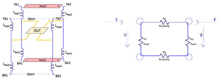
With very low impedance PDNs, especially when we do not have access to through via pairs connecting to the power planes, the definition of impedance gets complicated. Take for instance the four vias that we use for landing our probes. Figure 2 shows a generic equivalent of four vias connecting to the power-ground plane pair(s), providing eight terminals to land the four probe terminals. Dependent on how we assign the probe terminals as ports and which surface pads we leave unterminated, the scheme captures all possible combinations of probing, including cases when we probe on the same via pair or on different via pairs (adjacent or further-away), from same side or opposite sides. Figure 2 shows the case when both probes land on the same via pair, one on the top, one on the bottom, with same +/- terminal assignment, called STRAIGHT orientation. As it was pointed out in [2], with sub-milliohm impedance target values, the horizontal plane and cavity impedance creates noticeable attenuation even at very close separation, creating significant attenuation even between adjacent via pairs.
Devices Under Test
Two boards are used in this work. The first one is a test board developed for the IEEE Electrical Packaging Society (EPS) technical committee on electrical design, modeling, and simulation (TC-EDMS) [7]. The second board used for this investigation is a production board for high-power ASICs for ML/AI workloads, referred to as the “Production board” below. It will be discussed a bit later in this paper.
The board (‘IEEE board’ in the following text) answers the need for an open-source PDN benchmark platform available to the vendors of simulation tools and vendors of verification, test and measurement solutions as well as for anyone who designs and validates PDN. This version of the IEEE board is not intended for high-frequency modeling, high-frequency correlation, or high-frequency laminate characterization. The IEEE board is designed primarily for wafer-probe connections, not for direct coaxial connection. The PCB has six board sections with different targets of analysis. This paper focuses on two of them – Section 6 with calibration/reference structures and Section 2 with via arrays connecting to one power-ground plane cavity and allows us to examine the PDN behavior for typical device PCB connections.
The IEEE board is a 6-layer PCB, 10”x7.5” in size, divided into six identical-size rectangular areas, called sections in this paper [7].
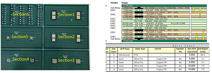
Each rectangular section has full planes on all four internal layers within and only within their own boundaries. The planes are 4.925” x 2.425” in size. This makes a cavity made by the L2 and L3 on the upper part of the PCB and another cavity made by L4 and L5 in the lower part of the PCB. These cavities mimic the VDD/VSS distribution used in application boards. The TOP and BOTTOM layers are pads only. There are no passive or active components, nor any connectors. The IEEE board stack-up, used for the first build, is shown in the PCB fabricator drawing in Figure 3. As visible in the figure, the IEEE boards were built with the same kind of laminate throughout all the layers using EMC EM-827, which is considered to be equivalent to Isola 370HR, a popular low-frequency laminate. According to the vendor data sheet, the dielectric constant and loss tangent at 1MHz for 50% glass-resin ratio is 4.8 and 0.018, respectively.
The IEEE board was built with flash gold surface finish. The exposed dielectric on the surface is covered by the customary green solder mask. Since the IEEE board is primarily for lower-frequency PDN tests, the solder mask has very little influence on the performance. To help locate various structures during measurements, there are silkscreen on the top and bottom. In the IEEE board file, each group of vias has a reference identifier and the vias have pin IDs assigned as will be shown in the following figures. Finally, the surface has a thieving pattern that covers all unused areas, again expected to have negligible influence on the electrical performance in our case.
Description of the IEEE Board Section 6 (Reference Structures)
The IEEE board Section 6 is a reference section, made of simple structures having two or four vias connecting the inner planes using the same via technology that we have in the board sections 1 through 5. The intention is to provide simple structures for convenient measurement and simulation calibration. Most of the reference vias connect intentionally to the same planes, which allow us to analyze short and long via loops, without the added complexity of a plane cavity. As shown in Figure 4, the reference via arrays in the IEEE Board section 6 are arranged in five columns, corresponding to the via pitch and configurations of the other five IEEE board sections.
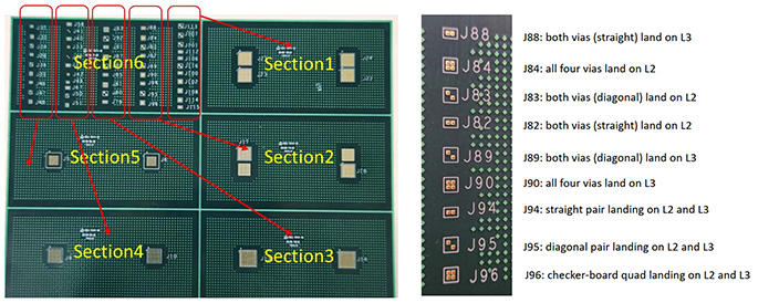
An example usage of this section of the IEEE board is shown later for the 4-pin via array of J84 which will be measured and simulated in different configurations. The four vias in J84 can be considered a subset of the arrays in IEEE board section 2, the difference being that all four vias in J84 are shorted on L2, while the IEEE board section 2 contains much bigger current loops. Even though we have only four vias in the group, this structure, just like several of the other reference via groups, offers many possible permutations to simulate and/or measure as discussed in relation to Figure 2. J84 was selected because it helps us bound expectations as it contains both the shortest possible local via loop from top to L2 as well as the longest possible via loop from the bottom layer to L2.
Description of the IEEE Board Section 2 (Via Array)
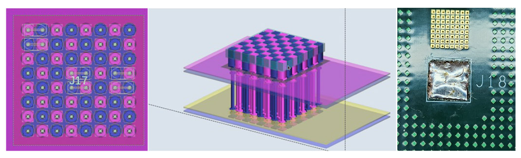
As shown on the left in Figure 5, in section 2 of the IEEE board there are four 8x8 via arrays: J17, J18, J19 and J20. J17 and J18 connect to the L2-L3 plane cavity close to the top of stack-up, and J19 and J20 connect to the L4-L5 plane cavity, close to the bottom of the stack-up. The via pitch is 1mm (approximately 40 mils).
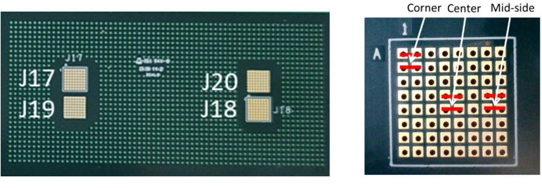
On the right of Figure 5 is the top view of array J17 with the port assignment used in this paper for simulations and measurements. Pin A1 is connected to GND in all arrays. From there the pins follow a checker-board pattern and alternate between power and ground.
Note that because all four arrays use through holes, all four arrays are accessible from both the top and bottom side. The IEEE board Section 2 offers the opportunity to probe via arrays that are connected to one plane cavity only. Moreover, as we are dealing with through vias it allows us maximum flexibility to probe in all possible measurement configurations of the four vias and two probes. To name a few obvious choices, we can probe at the selected via pair from top to bottom, at adjacent or more distant neighbor via pairs from the same side, either top or bottom. The spatial effect can be looked at by probing the structure at different locations, for instance at the corner, center and at the mid-point of a side. The locations shown in Figure 5 also give the possibility to get transfer parameters between more distant locations.
If we probe power-ground vias in the via arrays with nothing attached to the board, we probe a non-terminated plane cavity, which represents capacitive reactance at low frequencies. At high frequencies, where the modal resonances of the planes develop, we could also collect information about the dielectric properties. If we limit ourselves to frequencies below the modal resonances, we need a shorted structure so that we can assess the resistance and inductance of the structure. We can solder a shorting plane over the second via array on the planes, in this case J18, but it may require a professional BGA soldering station to do it properly and repeatably. Alternatively, we can create removable shorts by clamping a carefully flattened copper sheet, cut to the proper size, over the entire via array of J18. To make sure that the connection is repeatable, we can apply silver paste on the shorting copper sheet. Both approaches were used in the results presented in this paper as shown in Figure 13 and Figure 18.
Description of the Production Board
The production board discussed in detail later in the paper was chosen due to its low-impedance design impedance target (10’s of μΩ) to accommodate a high-power ASIC. This board was included in this paper for two reasons. First is to demonstrate in real-world applications how the tip coupling between the measurement probes themselves can add additional inductance, masking the actual PDN impedance. Secondly, the board raises questions on how to interpret the results from a VNA measurement when we consider how the PDN will actually get excited when there are high-current devices with a large number of power and ground connections over a larger pin-field area. With the low lateral plane impedance design targets, the number of vertical connections to these planes matter, i.e., the number of connection points within the pin field will produce different impedance values. Questions then arise: How do we interpret these different impedance values? How do these different impedance values compare with the two-port frequency-domain measurement obtained?
The board used for this investigation is a production board for high-power ASICs for ML/AI workloads. The production mezzanine card measures approximately 4-inches high x 8-inches wide with an ASIC centered in the middle of the card horizontally and spanning the entire vertical height of the card. There are 20 layers in the stack. Although there are several power rails on the ASIC, this study focused on the current-hungry core power rail requiring approximately 1kW of power and consisting of approximately 550 supply pins. The impedance target for this rail is approximately 45μΩ.
The setup for these measurements is consistent with the one used for Section 6 of the IEEE board. Probes were placed 4mm (about 0.16 in) from each other to reduce the probe coupling. However, this separation means we are now measuring transfer impedance (not self-impedance) and to match with the simulation, port placement should match the actual probe locations. See [7].
Simulation Setup
Capturing very low coupling with an EM field solver can be a challenging task. Several aspects impact the quality of the results: the choice of solver, extraction settings, boundary conditions, and frequency sweep amongst others. For this study we have used almost exclusively a full wave 3D FEM solver [8]. Normally, for power integrity related studies we tend to opt for a hybrid solver like [9] however in this case we are interested in the detailed behavior of the transition from the pads into the planes and so the starting point should be to select a solver that discretizes the entire geometry, including the dielectrics.
Current distribution throughout the layout is governed by what provides the lowest overall impedance. At DC, it can lead to interesting and relatively complex current flows within the layout such as that shown in Figure 7 which emulates a lab resistance measurement setup where current is injected between two diagonally placed vias on one side of the IEEE board and the voltage is measured on the same pin pair on the other side. The picture shows the current density on the shorting plane around J84. The current density on the inner part of the driven vias pairs is more than twice that of the outer side of the via barrel (NW/SE corners).
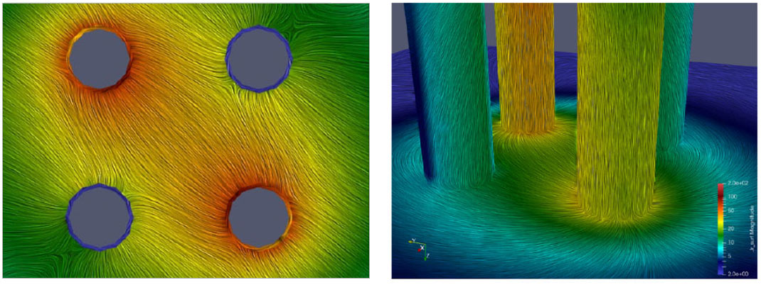
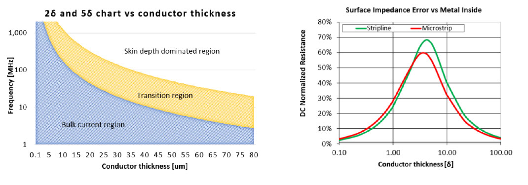
On the ground plane above, current varies along the plane itself (x-y), but for a given x-y location the current at DC is distributed equally throughout the height of the copper except around transitions such as from plane to via. However, as we increase frequency the current will start being pushed to the outer surfaces of the conductors due to the skin effect. For typical PCB conductivities and characteristic thicknesses, the transition between the DC and AC region occurs somewhere in the 10-100 MHz range which is within the range of interest for this study, so caution needs to be applied in the field solver, with respect to how the metals are meshed and how frequency data points are sampled (especially for adaptive sweeps). Figure 8 shows the transition frequencies for 58MS/m conductivity as a function of conductor thickness.
In addition, a typical example of fitting issues comes from using surface impedance boundary conditions, and even if fitting is done between the DC point and the skin-impedance boundary an error can be accumulated in the transition band. Although we are looking at plane behavior in this paper, a case where it is relatively easy to calculate analytically the mismatch between surface impedance boundary and actual current distribution uses transmission lines and is shown below in Figure 8. The graph shows the error in the transition band from using a skin-impedance surface boundary model, showing that a peak error somewhere on the order of 60% can be incurred. An experiment was made using J84 @ 10MHz (a launch with short on layer 2 in section 6 of the IEEE board) and it was found that a similar level of error was accrued in this case also. Thus, meshing inside the metals will be critical for low impedance characterization, but because it's numerically expensive, the option should only be used if absolutely required.
The transition band can also impact the quality of results from a typical adaptive frequency sweep, so similar care should be applied here. If the transition band is not sufficiently sampled an adaptive sweep can lead to drastic jumps in s-parameters below the ΔS limit (discussed below). Keep in mind however that S-parameters below the ΔS limit are not guaranteed accurate and even if, only then for frequencies at which the mesh is adapted. In this study the mesh was adapted at 10MHz and 2GHz (although the high frequency adaptation is not required for the data shown in this paper).
ΔS is probably the most common convergence criteria used in FEM solvers and is the key metric in determining the accuracy of any of the extracted results. As with the reflection calibration loss level in measurements, ΔS sets the lower limit to which results can be trusted, or in other words the noise floor. Without going into too much detail, a ΔS of 0.01 would mean the extraction results are accurate down to -40dB but only at the adaptation frequency (the frequency where the mesh is generated). As the s-parameters approach the -40dB limit uncertainty increases such that a simulated S11 of -40dB is actually -40dB±6dB. The reason can most easily be understood by recalling that we are dealing with vectors – we have a signal and a noise vector. As the signal magnitude approaches the noise floor the uncertainty grows exponentially, particularly for phase. This topic was discussed in more detail in [10].
Thus, limitations in the simulation parallels some of the limitations we have in measurements, but with at least two exceptions important for this work. We are measuring PDN structures that are almost a short circuit at low frequency, and therefore the reflection coefficient cannot be used for deriving the DUT impedance with sufficient accuracy as was explained in [4]. Also in measurement, the probe impedance is fixed to 50Ω (25Ω effective load in the 2-port method). If we could improve the noise floor and lower port impedance, we can further improve the measurement accuracy. Essentially neither of these limitations are present in simulation, but there is still finite mathematical accuracy. A typical practice is to lower port impedance down to 1Ω (or lower) to better utilize the numerical resolution.
In simulation, result accuracy is typically ΔS limited (as it impacts absolute result accuracy and extraction time) and not limited by numerical noise. Essentially this means that we can get well behaved s-parameters below the ΔS limit. However, if you compare two different extractors there is no guarantee the results will be identical below the ΔS limit. It was found in this work that the s-parameters, inductance, and resistance values from the calibration section 6 of the IEEE board converged to a few percent with ΔS = 0.005 in the first 3-4 iterations while, because we see more global effects in IEEE board sector 2, convergence required 7 iterations with the same ΔS setting. Now, although it is tempting to try to make generalized conclusions about this it is important to mention that there is an interdependency between the ΔS metric and how much the mesh is refined between iterations, so rather than making general claims the user should do their own convergence studies.
Manufacturing related aspects such as etching effects can be important details to consider too for these kinds of investigations – in this case we are mostly concerned with ensuring we have the right stack up as per the cross-section report, but for more complex geometry than what is being inspected on the IEEE board, things such as the etching process can lead to increased resistance. This topic was discussed extensively in [11].
The final topic to discuss here is the method of excitation of the DUT structures in simulation. We will be comparing against measurements that are either done with probes embedded in the measurements (Ecal/Mcal) or wafer calibrated probes both potentially including uncalibrated coupling between the probe tips. In simulation, we are not in the same way DUT access limited, and we can make the ports electrically small in the frequency range of interest (<λ/40) so using lumped ports should contribute very little additional parasitic coupling. This was tested for a few of the structures in section 6 of the IEEE board. No noticeable change in the extracted inductance was found when de-embedding the lumped port parasitics. For comparing directly to measurement, we can either include a full 3D probe model in our simulation at the expense of simulation time or we can de-embed the probes from the measurements. The latter solution is ideal as what we are trying to do in measurements is to characterize the DUT. The purpose with this kind of examination is to find out how big an error we are making due to the physical limitations of the measurements as well as understand the level of variation we can expect due to PCB manufacturing and materials variability and the solver settings.
Probe Models
Probe models were generated from our wafer probes for analysis of the different calibration strategies: a SOLT coaxial calibration to the end of the cables and a SOLT calibration to the tips of wafer probes using a calibration substrate [17]. The SOLT calibration to the end of the coaxial cables was completed using an Ecal [15]. Calibrating using only an Ecal to the end of the coax cables creates ambiguity around the impact of the wafer probes on the measurement error and quality. We decided to model the probes and evaluate the impact of de-embedding them from Ecal calibration-based measurements and clarify the impact of not calibrating out the probes from measurement.
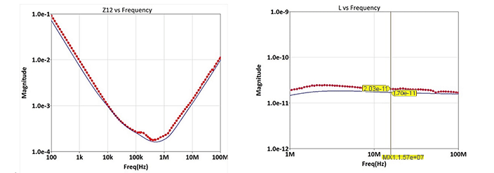
The RP-GR-121510 probes [13] intended to be used in the measurement setup were each measured using a one-port measurement in an OPEN, SHORT, and LOAD configurations. A simple W-element transmission line model was fitted to these measured s-parameter datasets. The lengths of the probes were measured using a digital caliper to be approximately 36mm. The Dk of the probes’ dielectric material was set by fitting the model to the quarter-wave resonance of the s-parameter measurement corresponding to the open configuration. Lumped inductance was added to the end of the coax model such that the full series coax model with lumped inductance give an impedance profile matching the quarter wave resonance of the shorted configuration. Finally, the resistance per unit length was tuned to match the dampening of the measured s-parameters’ Q’s. The final fitted model is shown in Figure 9 and comparisons between the measured probe s-parameters and fitted probe model are shown in Figure 10. The fitted probe model matches the OPEN, SHORT, and LOAD s-parameter measurements well so the team moved forward with these models of the wafer probes.
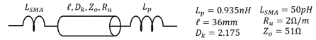
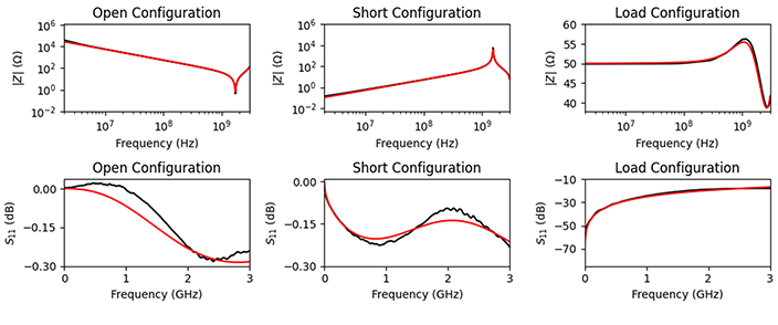
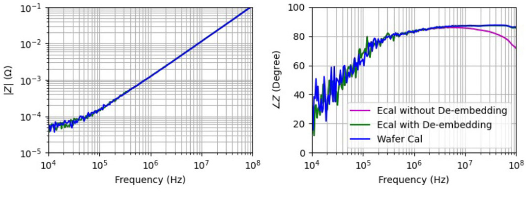
Figure 11 below shows an impedance profile measurement using wafer probe calibration to the tips of the wafer probes (blue), a measurement of the same impedance profile using Ecal calibration to the end of the coax cables without de-embedding the wafer probes (purple), and the post-processed Ecal based measurement after de-embedding the wafer probes using the fitted probe model described above for each probe. The impedance measured was that of J84, a shorted plane structure on the IEEE board with both wafer probes connecting from the bottom side of the structure, oriented in a “straight” configuration with one another. There is no noticeable difference in the impedance magnitude up to 100MHz between either calibration strategy. The phase difference between the wafer probe calibrated measurement and the Ecal measurement before processing diverges in the resolvable region around 10MHz by approximately 1 degree and then by 15 degrees at 100MHz. After post-processing by de-embedding the wafer probes, the phase difference is less than 0.2 degrees at 10MHz and less than 1 degree at 100MHz. While the de-embedding improves correlation with the measurement calibrated to the tips of the wafer probes, having 1 degree phase difference or less at 10MHz allows us to conclude that up to this frequency the wafer probes do not contribute sufficient error. Up to 10MHz we can confidently take impedance profile measurements using coaxial calibration to the end of the coaxial cables and neglect the contribution of the wafer probes to the measurement error.
Measurement Setup and Calibration
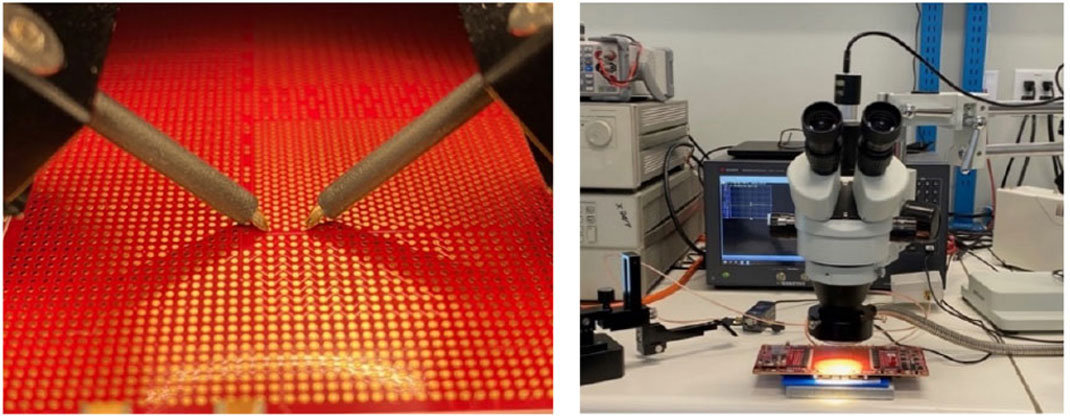
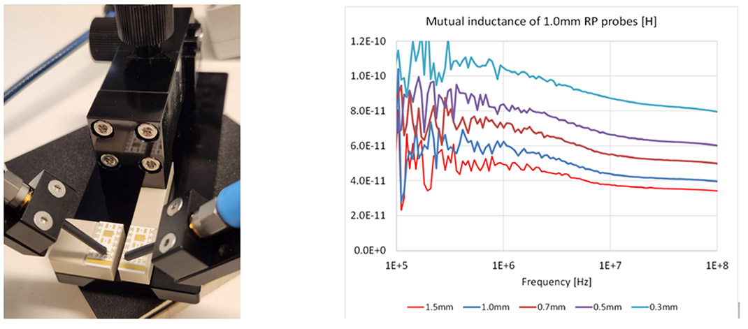
Spatial effects in PDNs show up at all frequencies relevant to power distribution, which may cover DC to many GHz and can include time domain noise, frequency domain impedance or radiation measurements. In this paper we focus on low-impedance PDN structures and limit ourselves to low frequencies, way below the lowest modal resonance frequency of the PDN. In frequency-domain impedance measurements these conditions call for a two-port shunt-through connection scheme with provision to suppress the cable-braid loop error. To allow for full two-port calibrations, the two-port VNA with low-frequency extension and Impedance Analysis option was used [12]. Two 48-inch-long N-SMA cables [13] were used to connect to pin-type PI probes [14]. Some of the measurements did not connect the two probes directly together, for instance when probe coupling was measured with both probes landed separately on shorting strips. In those measurements there was no need to suppress cable braid loop error. In all other cases a common-mode toroid was used (like [15]) to increase the cable braid inductance and by doing so push the braid R-L cutoff frequency outside of the measurement frequency range. In our setup a home-made common-mode transformer was used with SMA connectors. Figure 12 shows the fixture and extracted data of inductive coupling between two RP-GR-121510 probes as a function of polarity and distance. The custom wafer-probe positioner accommodates two calibration substrates, one at a fixed location and another that is adjusted in XYZ directions in fine increments.
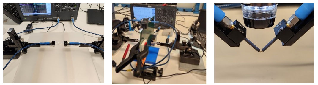
Calibrations were done in three different ways. For quick calibrations an economy Ecal unit was used [16]. Note that the Ecal unit allows a maximum of -15dBm source power during calibration. However, after the calibration we should change the source power to at least 0dBm to provide a good noise floor. For more accurate calibrations a mechanical calibration kit was also used [17], which does not have restrictions on the VNA source power, so calibrations and measurements were used with at least 0dBm source power. These two coaxial calibration options allowed us to do full two-port SOLT calibrations to the end of the cables (SOLR is not available on this VNA model). This means that all measured data included the two probes as well. The probes were characterized separately with wafer calibration substrates [18]. The probes were landed on OPEN, SHORT and LOAD and their responses were measured, making sure that the other probe was far removed. 2x THRU formed by the two probes was also captured in different configurations: touching the probe tips in the air using the default 45-degree probe attachment interface; touching the probe tips in the air using a 0-degree (in-line) probe adaptor and touching the two ends of the floating two-via THRU structure, J115, in the IEEE board. The latter two options are expected to eliminate the probe-tip coupling during the THRU calibration step. The setup also requires X-Y-Z positioners for the probes and the vision system, preferably with two cameras so that each probe can be followed without repositioning the camera. The photo below shows the instrumentation and setup with all their listed elements.
Instrument Setting
The frequency range was optimized to capture the important signatures of the DUT. Quick, cursory measurements were run in a wide frequency range and based on the result the final sweep range was set. In many cases it was 100Hz to 10MHz logarithmic sweep with 10Hz or lower IFBW. Some quicker measurements were taken with 10kHz to 100MHz logarithmic sweep with 100Hz IFBW. Note that since the common-mode choke and the cabling had some inherent resonances around 30-40MHz, even though after calibration the data looked good, the frequency range above 10MHz was not used for correlation purposes. Finally, to allow the maximum available resolution of the model, the probe characterization was done with linear sweep in the full 3GHz frequency range with 1500 points and 2MHz frequency increments.
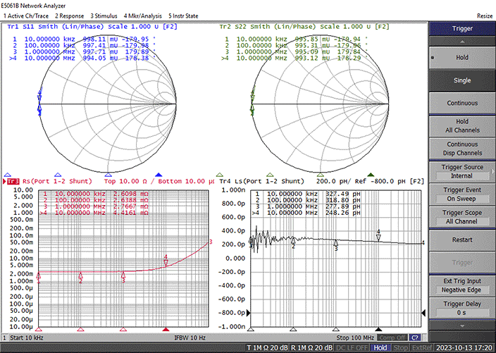
It is equally important to set the display of the instrument properly so that it can give us the maximum immediate feedback during calibration and measurement. For the chosen DUTs, which are essentially R-L circuits at low frequencies, it was found to be useful to split the display into four quadrants, display the reflections on the top on Smith charts and the extracted R and L on the bottom. This entire project assumes that the DUT has no coaxial access and therefore we need to land on DUT features with wafer probes. The Smith charts allow us to see if both probes are properly landed such that the sweep starts from the -1 point. This visual feedback is very important during wafer-probe calibration, when we must go through seven independent probe landing and if any one of them is compromised, we have errors baked into any successive measurement result. The bottom two charts display the R and L values of the parallel self-impedance, extracted from S21 alone. Note that for highly reflective impedance values calculating the PDN impedance from the Z matrix would contain significant errors, because the self-reflection terms of the measured S matrix would be highly inaccurate. Figure 14 below shows this display setup.
Reference Measurements
While the IEEE PDN board [7] was created in such a way that it is not pushing the dynamic range of the instrumentation too hard, it is still a good idea to run a few reference measurements after calibration.
For low-impedance measurements the most important thing is to establish the noise and error floor with the given setting and accessories. While we could just disconnect the cables and record the trace noise of the VNA, this is not enough; in practice it is very hard to utilize the full available dynamic range of the VNA. The main limiting factors are the cable braid resistance error, the cable braid crosstalk and cable resonances. To get all these limitations on the screen, we need to replace the probes with back-to-back shorts and position the cables in the same way they will be laying around during measurement. Running a sweep will show if there is still any residual cable-braid error in our frequency range, and if there is any resonance and/or crosstalk associated with the cable braids. The two plots on Figure 15 show 5Hz – 100MHz sweeps with cases where all three errors are visible and after improvement. The orange trace on the left graph is the acceptable solution, where the cable-braid error is completely suppressed into the noise floor above approximately 300Hz. Blue trace on the same plot shows the reading without common-mode choke. There is no braid-crosstalk or resonance up to 100MHz. The blue trace on the right plot is a coaxial cable with worse shielding, exhibiting significant crosstalk and resonance above 10MHz. The orange trace on the right plot illustrates what happens with insufficiently torqued connector(s): at low frequencies it increases the return path resistance error.
![Reference measurements with back-to-back thru shorts showing residual cable-braid loop error, braid crosstalk and braid resonance. [Left] Note the benefit of the common-mode choke at low frequencies. [Right] Both measurements include the common-mode choke.](/content/dam/cadence-www/global/en_US/images/resources/whitepaper/designcon-2024-figure-15.jpg)
To reduce the cable-braid loop error, we either must use a common-mode choke with higher inductance, or not include the very low frequency range in the measured data. We could use DC coupled amplifiers as well, but those would prevent us from doing full two-port calibrations. The cable braid resonance can be suppressed by lossy ferrite clamps on the cables. And finally, the cable braid crosstalk can be reduced by moving the cables further apart and/or covering part or the entire cable length with absorbing ferrites.
Measurement to Simulation Correlation
IEEE Board Calibration Structure Examination (Section 6)
The first portion to be examined on the IEEE board will be the test structures in its section 6. The relevant connections were shown in Figure 5. As the section 6 structures are used for sensitivity studies and calibration, we will concentrate on setups that are identical to a typical PDN scenario, i.e., where we have something that looks like a short circuit. The connections that provide a short circuit to the same plane remove any complications caused by plane cavities and thus will emphasize the impact of local effects around the launch itself. We will examine J84 in the following discussion as it provides the shortest as well as longest via launch and therefore, we can bound our expectations for what we will see in other sections of the IEEE board. J84 exhibits the following characteristics:
- Relatively short path from probe landing on the top side with correspondingly low inductive coupling between the vias
- Long coupled vias when probing on the bottom side, allowing us to examine the impact of via-to-via coupling and the impact of using straight probing vs flipped probing configurations
- Isolated probes – configuration 1: through one via pair, however common most overlap of current paths from via out to the plane which could potentially increase coupling
- Isolated probes – configuration 2: probe on top on one via pair, and other probe on the adjacent via pair on the bottom side. This configuration would minimize overlap of current paths from the vias onto the plane
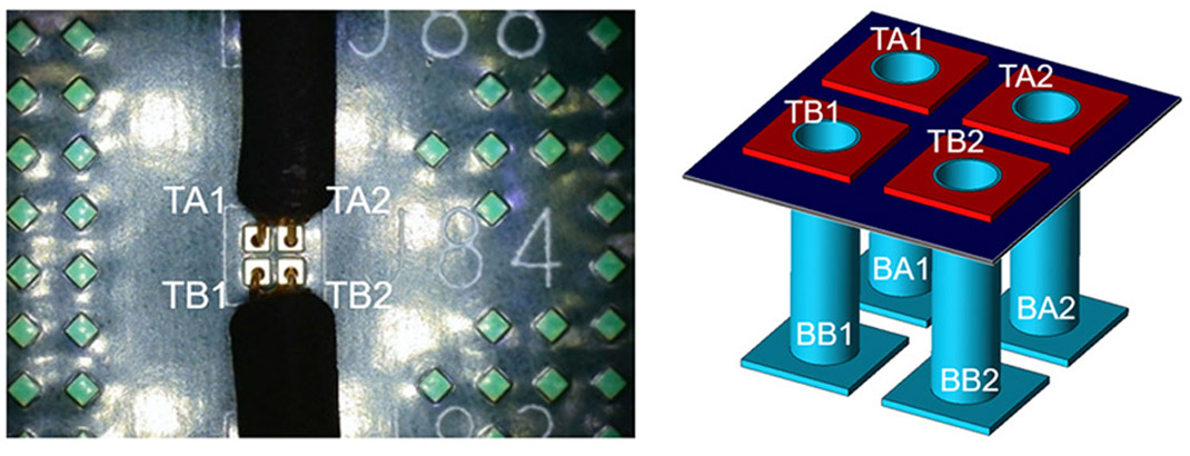
For clarification, referring to the picture below, configuration a is measured by putting probe 1 on TA1/TA2 and probe 2 on TB1/TB2, configuration b would have port1 on BA1/BA2 and probe 2 between BB1/BB2. Configuration c measures e.g., TA1/TA2 to BA1/BA2 and finally configuration d has probe 1 e.g., on TA1/TA2 and probe 2 on BB1/BB2. Note that the leading T or B refers to TOP or BOTTOM, respectively.
Below shows results from both measurements and simulation. The measurements were calibrated using a mechanical calibration kit [17] which implies that the probe tip coupling is included. The measurements were done both with straight and flipped probe configurations. The extractions were done using the settings discussed earlier and using lumped ports to get an idea of the "layout only" parasitics. Resistance and inductance comparison is done for both through, bottom and top side probe placements. Straight probe configuration is shown in blue, flipped in red and average of the two in yellow and finally simulation results in green.
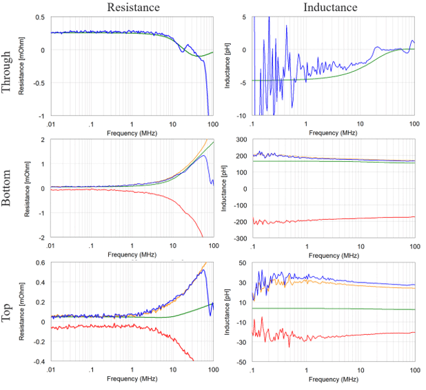
Overall, we see inductance and resistance trends being quite well aligned, but there are some obvious differences that become visible, especially for the resistance values when probing on the same side of the board. We see bandwidth limitations in the measured value, especially when measuring the very low values on the top side where we have the shortest via stub. Given the uncertainty in the characterization of the board geometry, tolerances on materials, measurements, and simulation setups on a first glance the correlation seems pretty good.
The table below summarizes the findings. Because the straight and flipped probe configurations should average out to give approximately what we expect from the structure without having the impact of the probing configuration, the sign of the extracted values from flipped / straight configurations have been excluded in below.
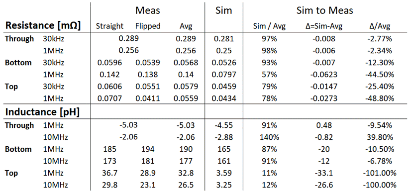
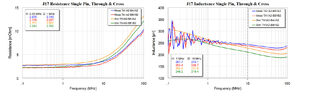
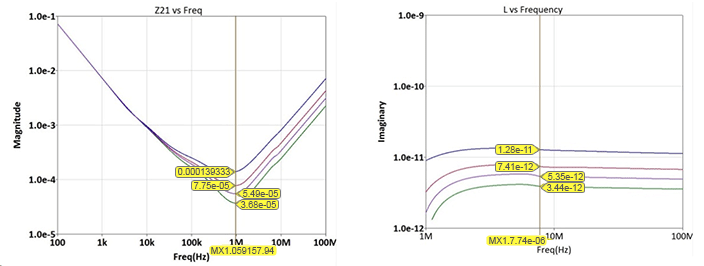
If we start with the through probing, i.e., the scenario we know minimizes probe to probe coupling, we generally see good agreement between the measurements and simulation for resistance with both having about 0.28mΩ resistance @ 30kHz. The inductance trends and values also are very similar from about 1Mhz onwards, whereas the low frequency measurement data suffers from noise due to challenges with accurate phase measurement at low frequency. Note however that the structure is not really inductive – as we would expect the through measurement is not dominated by inductive coupling.
As we move to the other probing configurations, we can see that the resistance correlation is significantly more bandwidth limited – there is around 2x result variation between measurement and simulation already at 2MHz for the top side probing, while for bottom side probing the 2x mark is reached around 15MHz. We also see that for resistance values below 100-200µΩ the measurement becomes gradually noisier which explains the relatively large difference for the bottom and top measured configurations. The behavior of the inductance is quite similar between measurement and simulation for the bottom side in behavior. However, for the top side measurement we have to compare with the avg value of the measured inductance (considering the sign reversal the average would be 3.35pH) in which case we are close to the simulated value. If we compare the inductance directly from the measurement in either straight or flipped configurations to the simulation, we see the inductance is around 30pH higher. In other words, 30pH is a rough estimate of the expected contribution from the probe coupling.
To summarize, as expected, two-port probing on opposite sides gives best predictability in the measurements, while for same side probing, we see that measurement limits the effective bandwidth over which we can expect results to correlate.
IEEE Board Section 2 – Distributed Plane Effects
Here we will be examining section 2 on the IEEE board. The simulation mimics the setup in the lab in terms of how the short circuit is introduced on one of the device sites, as shown below.
In PDN verification measurements we tend to measure the PDN with a two port VNA, this naturally limits the applicability of the measurement. When an actual device is connected to the PDN it can do so at many hundreds of locations, so the question arises how applicable the measurements are to verifying the PDN in such cases. The IEEE board is designed to mimic on a smaller scale such an application, in simulation we are able to group the pins in the array and measure the effect of the PDN at many locations.
Initially we start with individual ports at some set points in the design, these ports are placed both on the side that a device might be mounted as well as on the reverse side (mimicking measuring the PDN on the rear of the card). The simulation places a copper sheet at the location of J18 to simulate the low output impedance of the VRM. Similarly in the measurement environment a square piece of copper has been soldered to the board at the location of J18 for the same purpose.
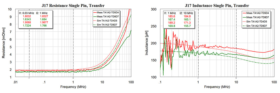
The resistance and loop inductance for both simulated and measured cases were extracted and compared for three positions, upper lefthand side, middle and middle righthand side on the top (component side) surface of the card corresponding to the configurations shown on the right of Figure 5.
The results above, show reasonable correlation of the PDN inductance to the measurement, as previously discussed, there is low confidence in the measurement data for extracting inductance at frequencies below 1MHz. There is some mismatch in the resistance prediction because the exact properties of the conductivity of the PCB materials and the short at J17 are not known.
Once the base line measurements and simulation correspondence had been established, we started looking at grouping pins at location J17. In a packaged component the PDN experienced by the die is as seen through many parallel paths and yet when the PDN performance is measured we typically do this using the 2-port method. A natural question is how the measured PDN impedance corresponds to that observed by the device itself with these multiple parallel paths.
For the grouping study we looked at several scenarios, in all cases lumped coaxial ports were placed ~0.5mm from the surface of the PCB by placing a PEC sheet to which all of the GND connections in the checkerboard array (32 pads) are connected. It is common for packages to have all the GND balls connected to the same internal package planes, and this is mimicked with this setup. Only the number and arrangement of the power connections were changed. To make the comparison to measurement, ports were placed on both sides of the PCB with the PEC planes at the same distance from the top and bottom surfaces.
Several cases were studied, the individual coaxial ports for the power connections were treated as a single port by using the port grouping option in the simulator. In this case equipotential grouping was used, but it is noted that equal-current grouping could have also been used but was not investigated. The cases mimic some typical scenarios within the limitations of the 8x8 array, for example the core supply of a package or the IO supply.
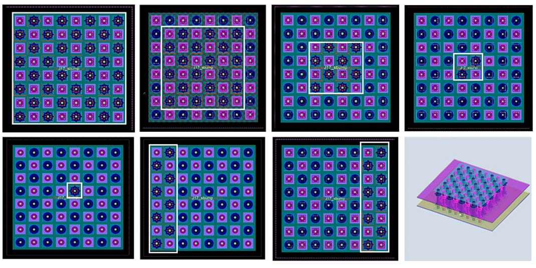
We will concentrate on the measurement point for thru connection at A1A2, that is probing top and bottom of this location in addition a thru crossed connection was measured (TA2A1 BB1B2). The measurements were compared to the centre grouped cases.
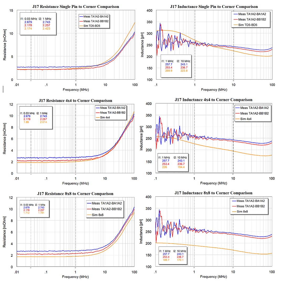
We observe, as expected, that as the number of contact positions increases both inductance and resistance decrease, and the simulations diverge from the measurement. Next, we looked at the transfer impedance between measurement points at J17, horizontally we might expect to see more loss because current would be drawn through the perforated plane areas in the via field. However, this effect was not really observed in the measurement, and this was confirmed by simulations.
Production Board Measurements and Simulations
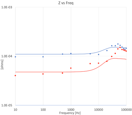
Simulations [19] were performed at the same probe location as was measured. The simulation consisted of a fully populated board less the ASIC including RLC models for the board capacitors. The goal with this initial simulation was to achieve correlation with the measured VNA data and then, using the same validated simulation environment and setup, parameterize the number of vertical connections to study how the number of excitation points impact the PDN impedance.
Figure 23 shows the correlation between simulations (blue) and measurement data (red). With an impedance target of worst case 75 μΩ in this application, we note that the impedance is higher in both simulated and measured results (160 μΩ) using a single measurement point or port location. The other observation is that the extracted PDN inductance is quite low because of the low impedance design target (17-20 pH). Comparing this inductance range to the top measurements in Table 1, we see that the coupling inductance ranges from 20-30 pH, potentially masking our PDN inductance.
The next step is to use the correlated simulation environment to help us understand how the excitation point impacts the PDN impedance by parameterizing port grouping. Specifically, we look at the following additional cases, which are shown in Figure 24 below:
- Grouping ¼ of the pins (Blue)
- Grouping ½ of the pins (Red)
- Grouping ¾ of the pins (Purple)
- Grouping all pins (Green)
Local VSS pins, within the grouped area, were included. Figure 24 shows that by grouping more balls, the impedance minima and inductance decreases significantly.
By extracting the real part at the impedance magnitude minima and the inductance above the series resonance frequency across the range of parameterized grouped pins, we see that the inductance and impedance minima follow hyperbolically decreasing values as we increase the number of VDD and VSS balls. We also see that the impedance target is now equal or lower than the design impedance target (37 vs 160 μΩ) with the BGA pin field grouped and uniformly excited. See below.
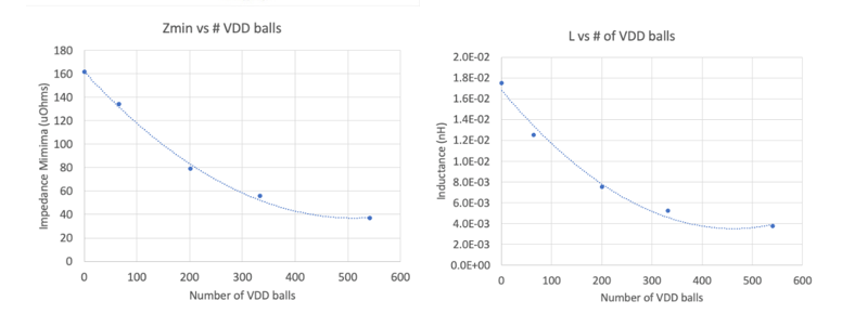
We note in the figures above that the scaling with impedance and inductance is relatively linear with a few numbers of via connections but flattens out as the number of via connections increases. We hypothesize that the scaling may appear to be linear under some circumstances, but heavily depends on the structure. Specifically, the linear scaling becomes asymptotically correct if the lateral plane impedance is much less than the impedance of each via accessing the plane AND we are at frequencies way below the limit where the spatial variation of plane impedance within the array would show up (aka full-wave effects). This condition occurs when we have very thin laminates and heavy planes with good conductors and the vias are skinny, inductive, and resistive. The other extreme is when the vias are very low impedance (short and fat) and the planes are high impedance (e.g., large plane separation, thin planes). The actual reality may be somewhere in between. The takeaways from these curves are two-fold: first, for these types of boards, two port measurements will not accurately measure your design impedance. Second, when designing these types of boards, we should be mindful to have sufficient connection points from the DUT to the board to minimize the impedance of the vertical connections.
We have shown that for certain structures, VNA measurement validation of the low impedance asymptote is problematic both in terms of probe coupling and a higher measured PDN impedance that may not be representative of the impedance as seen by the load. However, there are other approaches to validate the low-impedance asymptote using transient load testing [20]. Transient load testing involves connecting FETs across the pin field of the production board where the ASIC would be located. By controlling the current demand of the FETs, we can do a thorough characterization and analysis of the PDN in the time domain. The benefit of this method in terms of PDN validation is that we can now load the production board as if the ASIC was connected across the entire pin field, allowing us to derive the low impedance asymptote. Derivation of the impedance from the measured voltage and current step can be done in a number of ways. Here we share data on the same board measured and simulated above using a single-frequency sinusoidal current waveform which allows for direct computation of the impedance at that single tone using the measured voltage noise.
Figure 26 shows the low-frequency response of the same production board measured above with two different load line settings that were being tested with the VRM: 55 and 117 micro-ohms. The dots are extracted from sinusoidal current excitations (single tone) and the measured voltage noise whereas the solid lines are simulated using a simple RL model for the VRM. Specifically, the voltage was measured on the back of the production board in the pin field. This shows that we can use this method to extract low PDN impedances with full-chip excitation.
Conclusions
With high-current PDN impedance targets in the tens of micro-ohm level, the PDN validation becomes very challenging. Boards carrying large chips in the kW power range need large via arrays to connect the surface power-ground pads to the PDN distribution structure inside the board stack. Combined with the need for HDI board construction to satisfy high-speed connections, in many applications there may be no vertical through-hole via under the high-current chip, forcing connections of all validation instruments on the same side. Under these circumstances full-array transient tester fixtures provide the most relevant and accurate PDN validation. This, however, requires custom fixtures and circuitry, which raises the need for simpler and faster two-port impedance measurements with VNAs.
In this paper our main take-away shows with correlated data that with PDN impedances in the sub-milliohm level the impedance extracted from same-location top-bottom measurement can be significantly different from same-side adjacent via pair measurement even if the physical separation is in the order of a millimeter. This is compounded by the probe-tip and via coupling error added or subtracted from the actual DUT impedance. This error can be tens of pH inductance and tens of microohm resistance, potentially masking the DUT impedance. It was also shown that grouping many pins in an array yields simulated impedance similar to what we can obtain from top-bottom VNA measurement in the center of the via field (Figure 15, Figure 19, and Figure 21). However, pin grouping in simulation shunts out the lateral PDN impedance in the array, potentially resulting in unrealistically low simulated impedance. Additionally, it was also shown with correlated data that the phase shift and attenuation of wafer probes can be neglected below 10MHz and therefore a simple, more convenient and usually more accurate coaxial calibration can be used to the end of cables (Figure 10).
Acknowledgements
The authors wish to thank Heidi Barnes and every member of the IEEE TC-EDMS Packaging Benchmarks Committee, Patrick Davis and Jonathon Hendron of Cadence, Richard Zai of PacketMicro, Jean-Remy Bonnefoy, and Steve Duzan of Samtec for their help with this project. The authors would also like to thank Fadi Deek for his great work with the transient load calculations.
References
Author Biographies
Ethan Koether earned his master's degree in Electrical Engineering and Computer Science in 2014 from the Massachusetts Institute of Technology and has spent the last seven years as a hardware engineer at Oracle. He recently began his new role as a Power Integrity Engineer with Amazon's Project Kuiper. His interests are in commercial power solutions and power distribution network design, measurement, and analysis.
Kristoffer Skytte is an Application Engineer Architect at Cadence focusing on chip, package, board and full system analysis including SI, PI, thermal and EMC related challenges. He has held various application engineering roles for the past 20 years. As of late he has spent significant effort on examining differences between measurements and simulation and how these are shaped by what is being characterized and the assumptions made. Kristoffer holds an M.Sc.EE. degree from the Technical University of Denmark.
John Phillips is a principal application engineer with Cadence Design Systems. Prior to joining Cadence John worked at many different companies covering such diverse marketplaces as high end compute platforms and mil-aero. During his career he acquired a broad knowledge of SI, PI and EMC at chip, board and system level. John holds an MSc. Degree form Bolton University, UK. His current interests are SI/PI co-simulation and modelling for both serial and parallel interfaces.
Shirin Farrahi is a Senior Principal Software Engineer at Cadence working on SI and PI tools for automated PCB design. Prior to joining Cadence, she spent four years as a Hardware Engineer in the SPARC Microelectronics group at Oracle. She received her Ph.D. in Electrical Engineering from the Massachusetts Institute of Technology.
Julia Van Burger has been an SI/PI Co-op at Samtec for the past 6 months, as well as a 5th year student at Northeastern University. She is currently pursuing her undergraduate and master's degrees in electrical engineering, expected to graduate in 2024. She has a strong coding background and has transitioned her focus to power systems.
Joseph 'Abe' Hartman is a Principal Hardware Engineer focusing on system signal and power integrity at Oracle. Abe has worked as a signal integrity engineer at Amphenol TCS, Juniper Networks, and Enterasys. Abe also worked at General Motors. Abe holds a MS in Electrical Engineering from the University of Massachusetts-Lowell, a MS in Engineering Science from Rensselaer Polytechnic Institute, a BS in Mechanical Engineering and a BS in Electrical Engineering from Kettering University in Flint, MI.
Mario Rotigni retired after 45 years in Electronics. He was with the R&D Department of Magrini Galileo working on design of process instrumentation operating in very hostile electromagnetic environments. After designing Automatic Test Equipment for micro-controllers, he joined STMicroelectronics, holding various positions in the Engineering, Design, R&D inside the Automotive Product Group. Lately he was in charge of the EMC of Microcontroller and System on Chip for the automotive applications. He has co-authored 22 papers about EMC of Integrated Circuits for various Conferences and is currently a member of IEEE EMC Society.
Jason Miller is a Hardware Manager with Annapurna Labs. Prior to joining Annapurna Labs, Jason worked for Oracle leading a team responsible for signal and power integrity of ASICs on Oracle servers. He has published technical articles on topics such as signal and power integrity modeling and simulation, including receiving the Best Paper Award at DesignCon three times. He has co-authored with Istvan Novak the book "Frequency-Domain Characterization of Power Distribution Networks" published by Artech House and holds five patents. He received his Ph.D. in electrical engineering from Columbia University.
Gustavo Blando is a Senior Principal SI Architect at Samtec Inc. In addition to his leadership roles, he's charged with the development of new SI/PI methodologies, high speed characterization, tools and modeling. Gustavo has twenty-five years of practical experience in Signal Integrity, high speed circuits design and has participated in numerous conference publications.
Istvan Novak is a Principal Signal and Power Integrity Engineer at Samtec, working on advanced signal and power integrity designs. Prior to 2018 he was a Distinguished Engineer at SUN Microsystems, later Oracle. He worked on new technology development, advanced power distribution, and signal integrity design and validation methodologies for SUN's successful workgroup server families. He introduced the industry's first 25 μm power-ground laminates for large rigid computer boards and worked with component vendors to create a series of low inductance and controlled-ESR bypass capacitors. He also served as SUN's representative on the Copper Cable and Connector Workgroup of InfiniBand, and was engaged in the methodologies, designs and characterization of power-distribution networks from silicon to DC-DC converters. He is a Life Fellow of the IEEE with twenty-nine patents to his name, author of two books on power integrity, teaches signal and power integrity courses, and maintains a popular SI/PI website. Istvan was named Engineer of the Year at DesignCon 2020.